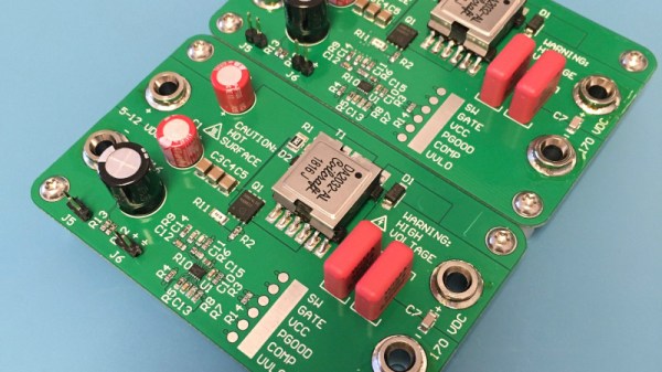
It is tempting to think of analogue and digital domains as entirely distinct, never to touch each other except like a cold war Checkpoint Charlie, through the medium of an ADC or DAC. In reality there are plenty of analogue effects upon digital circuitry which designers must be aware of, but there is one field in which the analogue and the digital are intricately meshed. Switch mode power supplies use digital techniques to exploit the analogue properties of components such as inductors and capacitors, and can be astoundingly clever in the way they do this to extract the last fraction of a percent efficiency from their conversion. Thus their design can be something of a Dark Art, so it’s always interesting to have a good read explaining some of the intricacies. [James Wilson] has built a flyback step-up converter to power Nixie tubes, and his write-up follows the whole process in great depth.
This type of converter seems at first glance to be a simple step-up design with a transformer that has a primary and secondary, where in fact it relies on the collapse in magnetic field during the off period of its duty cycle to provide a spike in voltage and thus a step-up beyond that you’d expect from the transformer alone. The write-up takes us through all this starting from a theoretical perspective, and then goes further into the realm of component selection and the effects of component properties on the waveforms involved. If you have ever battled ringing in a switch mode power supply you may recognise some of this.
If this field interests you, then there is probably no better place to send you for a start than Jim Williams’ 1987 app note 25 for Linear Technology: “Switching Regulators for Poets“.


