We’re suckers for some retro electronics here at Hackaday, so we were fascinated when Daniel Valuch wrote to us with some pictures of his findings in his CERN lab’s archive. He works on Linear Accelerator 3, which has had an extended downtime after many decades of continuous operation, for major upgrades and overhauls. Part of the upgrade involves the removal of electronic assemblies dating back as far as the 1970s, and he’s shared his fascination with them as he trawls through dusty filing cabinets in the lab basement.
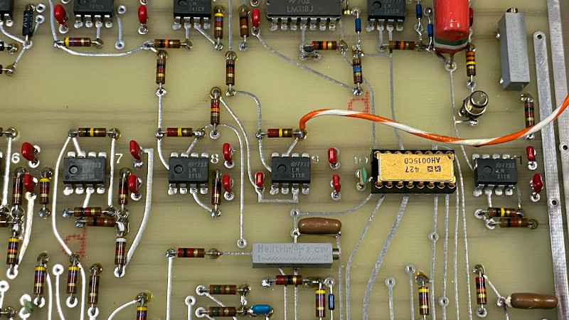
What it reveals is a world before the CAD and microcontrollers we know, instead here are circuits using the electronic building blocks of logic gates, discretes, and op-amps. PCBs are laid out not with the KiCad that CERN are famous in our community for today, but on acetate, with transfers and tape. A ground plane is even hand-carved from a red sheet. Oddly though it isn’t a world without CNC, because in the pouch with a design from 1974 is a roll of punched paper tape. If you have ever pondered the “Numerical” in “Computer Numerical Control”, here are the numbers in physical form.
For those of us who were trained in this type of electronic design, the convenience of a PCB CAD package and a professionally-made PCB at the click of a mouse is nothing short of miraculous. But seeing personally laid boards of this quality reminds us that seeing the hand of the designer in them is something few engineers today (with the possible exception of Boldport) manage to recreate.


“…but on acetate, with transfers and tape.”
Ah, the good old days. Any wire-wrap?
I started my career at CERN in 1984 doing exactly that: building prototypes with wire wrap…
To this day I think of PCB’s as art.
They are art.
At lest, they should be.
In days of old when knights were bold, and rubylith ruled the land….
I do not miss doing layout by hand and cutting rubylith for boards or for silicon. Not at all.
Then again, I still have call at times for hand layout and cut, but in a much different context (ong story short, when you reach a scale of 1 to 20m, time and cost often make hand layout and stencil-cutting the economical option)
Intrigued. Can you give us a hint? Maybe billboard displays?
Large ships.
Largest I have done in the last few years was 80m long, 1.5m high lettering for an in-service re-flag (PRC owner, reflagging to USA). Layed out and templated three sets at that scale (bow-port, bow- stbd, stern), templates and layout aids for company logo at 3m tall for the stack, class marks for the sides, waterline and load line markers, stencils for lifeboats, rescue gig, loading marks, safety marks, even emergency exits. A few were cut on site with a hobby knife when the client realized they missed something. Had to meet deadline, and I can cut them faster and cheaper than a commercial source can, then courier them, then get them to the vessel. Especially when the deficiency is found at 10PM on a weekend. Laser cutters have taken most of the small stuff the last few years, for non-exceptional cases.
Made a lot of money on that job. Much easier than my nominal job for the company.
Those LM311N are commercial temperature range, plastic packaged parts. The soldering on the leads and pads doesn’t look very good; in many places the fillet is poor and in some places there appears to be flux residue. This is not an example of high quality electronics.
It survived 40+ years like that, so you’re looking at the wrong things.
what is your definition of the word “quality”???
If you don’t realize the folly of attempting to analyze the quality of a PCB from a single low-resolution image then there is really no hope for you. With the crappy resolution of these pictures the artifacts you see could be just about anything.
By my definition this stuff is very high quality, I’m looking at the lack of downtime, the long service life, the accuracy of the obtained results. “The proof is in the pudding” From the photos this gear is in places also frequented by humans, and subsequently under climate control, so the extended temperature range parts are unnecessary.
The ability to stand time is not a metric of quality, only luck.
Roman roads.
One card, OK, maybe luck. A whole rack full running for 40+ years? Not so much.
We don’t know how many times they had problems that had to be fixed, especially near the beginning of that period.
Chris,
I agree, I was still very surprised the flux was not washed off. The board is photographed, as it was installed and running for 4 decades.
The post is more about appreciation how people designed circuits and printed boards during that era. The PCB artwork is simply perfect, the amount of effort which went into making these things is mind boggling.
It is also likely that some of the flux left behind could be from rework. Some of the solder joints (e.g. resistors) have notably more solder than others. It is on those solder joints that have resin residues.
The layout isn’t too bad considering that it is done without iterations like I usually do in CAD.
In those days the flux was colophonium, non corrosive and non hygroscopic.
Nowadays you have that rohs water soluble crap that you need to remove after soldering.
Fortunately I have plenty of the lead and colophonium stuff left and never remove flux, except maybe for very HF stuff.
No corrosion or any bad effect even after 30 years.
Yah I’ve never worried about leaving rosin on. I think the only time I take it off is if it really blobbed between tracks or pads and I have to check there’s not a wee whisker under it.
You guys beat me to it. I was going to write the same thing. I never worried about cleaning rosin except high frequency analog RF work, or if the flux was aesthetically displeasing. I’ve got several big rolls of Kester solder in various gages that I bought in the 1980s on my bench that will probably last the rest of my life. I’m glad I have it.
I think the same.
in fact, the rosin/ colophonium was left there on purpose.
It acted as a protective layer, preventing oxidation and such..
Anyway, this perhaps is rather difficult to explain to those younger peoples here who grew up in nowadays prosperous days, where every kid can own lab equipment..
Back then, prototypes and small series productions were valued more than mass produced stuff. They were hand made and tested manually by humans, after all.
That white/orange stripe wire tacked on top of the pad for the 220K resistor instead of having its own through hole does not exactly shout, “quality!” It appears the LM311s are regular consumer spec and the discrete components are 5% tolerance. Maybe that is sufficient for the application and/or the components were hand selected and matched. Some of the solder on 741s looks like it might be cold joints.
I have some old Mohawk Data Sciences boards that appear to be hand laid out full of DTL in ceramic packages that are quite pretty. Also I have some old 1970s Burroughs boards that are quite artistic – lots of gold 40 pin ceramics, tantalum bypass capacitors and 1% resistors. I kept those boards just ‘cuz they look cool.
~~
Somebody mentioned wire wrap. My second co-op work assignment was to fix a piece of test equipment to exercise telecom equipment that RCA had built for the lab I worked for. The circuit was about 50 4000 series CMOS parts and various other components that had been about put together with wire wrap, about 80% of which had been done with slit-n-wrap. Slit-n-wrap is a continuous feed system that does not strip the insulation off the wires. Instead the wire gun scores the insulation as the wire is being wrapped. It works as long as operator holds the gun perfectly so the insulation slit contacts the corners of the wrapping posts. Unfortunately it is easy for the wire to roll as it wraps, putting insulation instead of metal against the post. That gave me a couple of days ringing out the connections and doing a lot of re-wrapping with pre-stripped wires and a good quality OK Tools electric gun.
At the time I lived on the north side of the Washington, D.C. area and the Metro was brand new. The Metro control system was breaking down almost weekly, and the trains would limp at 10 MPH or so on the sections without full control. One evening, the TV news was running a story about yet another Metro break down and they showed a technician opening a cabinet and it was full of wire wrap boards. I thought to myself – bet they used slit-n-wrap!
Exatamente.
They are soldered from the bottom. It the solder doesn´t completely suck to the upper side, that´s not an issue.
But there are also plenty of places where components are soldered on the top. That seems strange if the holes were all plated.
May be they are reworks for bypassing faulty plated through holes? Poor quality.
I see you’re to cousin to Instagram welders, Instagram solderers…
Count me in for that exceptions list. And also your old gurus who did their best in Eastern Europe during the communist era behind the Iron Curtain.
One of the pcb’s in an Olivetti Programma 101:
https://www.flickr.com/photos/simski/16039513546
This reminds me of what electronics was like when I first started working. Back in those days the stuff they used to remove the flux was much nastier than the flux itself. Rosin flux, when fresh, may be sticky and gooey, but it is very benign to most electronics, I worked on a few projects with high voltage where cleanness and meticulous lead dress were called for to prevent arcing and coronas, and I also worked on a couple things with crazy high resistances, and again they had to be meticulously cleaned of both flux and any oils etc from your hands. For about 99% of the stuff that came through, the cleaning of the flux was a combination of cosmetics and the fact that no one wanted the stuff all over their hands.
The holes are plated through, and soldered from the bottom. Hakuna matata.
No one criticised the fact that there are two trimmer potentiometers visible on the board – and a wire link that is clearly a mod. Perhaps you should reflect on the fact that this was state of the art in the early 1970s – and without the 40 years of electronics evolution of these hand manufactured pcbs you wouldn’t be clicking on your $200 laptops or cell phones now. Cut some slack please.
I had the pleasure of doing some undergraduate research at the Cornell High Energy Synchrotron Source last summer. They are in the process of upgrading many things but it was still great fun to see their control room full of discrete logic chips and blinken lights.
I still have a pcb from 70s taken from some sort of early computer with out of this world integrated chip with a square metal cover and you could actually see the logic gates .would like to share this if possible
Yeah before ASICs there was a medium scale* integration thing, using thick film or thin film hybrid circuit tech. One could buy dies of various building block ICs gates, OP amps etc and have them mounted on these printed substrates that may have had capacitors and resistors printed to them directly, or have had the forerunners of surface mount components. However with some techniques transistors could be printed and sputtered to the substrate direct. It’s fascinating stuff, combo of ceramics, vacuum sputtering work, photo and lithographic processes. I’ve got an old textbook for some University’s “Microelectronic Technology” course, from when it was bleeding edge early 70s, before it was obvious ASICs were the way to go. It’s all photostat and mimeograph stuff bound together, which unfortunately probably won’t scan very well/easily due to it being questionable quality in the first place.
* Nobody knew what the limits were in 60s or 70s when the papers were getting written and some refer to this kind of stuff as large scale integration, because you can get 50 transistors in square inch, woohoo, incredible density!!!
Technically the limits were different then, because limits are about what you can do versus what you can dream or theorize about.
Also notice, no 90deg truns in the lands. That was a design no -no with tape, as it could cause it to peel up. A 90 corner could get caught when putting sheets back in and out of the flat file draws……
Most of the time the original tape layouts were done 4:1 or 2:1 iirc (it’s been 40 years) to get better resolution.