We’ll be honest, we were more excited by Duke University’s announcement that they’d used carbon-based inks to 3D print a transistor than we were by their assertion that it was recyclable. Not that recyclability is a bad thing, of course. But we would imagine that any carbon ink on a paper-like substrate will fit in the same category. In this case, the team developed an ink from wood called nanocelluose.
As a material, nanocellulose is nothing new. The breakthrough was preparing it in an ink formulation. The researchers developed a method for suspending crystals of nanocellulose that can work as an insulator in the printed transistors. Using the three inks at room temperature, an inkjet-like printer can produce transistors that were functioning six months after printing.
The technology uses carbon nanotubes for the semiconductor material and graphene for the conductors. The addition of mobile sodium ions via sodium chloride to the insulating material improved the resulting transistor’s performance.
Of course, right now this isn’t a commercial technology, but we have to wonder if this isn’t something hackers could do. Modifying an inkjet printer isn’t hard to imagine. Preparing the ink may or may not be in the realm of the basement lab.
This looks conceptually simpler than the last electronics printer we talked about. Maybe you want your 3D printed semiconductors a bit less practical.


In this case, the team developed an ink from wood called nanocelluose.
A bit unclear what is meant here…
I’m prety sure that there’s no nanocelluose tree.
Likewise, they didn’t come up with nanocelluose itself, but rather a use for it.
So maybe you meant “an ink from a wood *product* known as nanocelluose”?
Well I dunno… maybe programming syntax will help. (In this case) (the team) (developed an ink from wood) (called nanocelluose). Then later, I mention that it existed before but not as an ink. I mean, I saw a sign today that said “Take the shuttle bus grocery shopping.” I could have complained they think I’m going to bring the bus in the store with me while I shop, but I’m smart enough to realize what interpretation they meant.
Sloppy editing ! copy-pasting your own typo ad nauseam
celluLose. Because it come from the celluLar membrane
Cellulose doesn’t come from the cellular membrane. It comeS from the cell wall. That’s why animals don’t have cellulose. We don’t have cell walls.
Yes, Al, your sentence is fine. It’s only ambiguous out of context, and if you know absolutely nothing about the topic. You’d probably have to be purposefully obtuse to make a mistake while reading it. Now, we could look at [If only words were easy]’s grammar and find plenty to complain about:
The first sentence the quote is lacking quotation marks, which make it seem like an incomplete thought. However you could not fix it simply by adding quotation marks, because we’d then be left with a subject with no predicate.
In the second sentence there no subject at all.
In the third sentence, he/she misspells the word “pretty.”
In the last sentence he/she places the question mark outside of the quotation marks, which is wrong in American English but acceptable in British English.
Throughout the comment, he/she places each sentence on a new line, but he/she is not making a list. That is wrong in every English speaking country that I am aware of.
If I saw a sign that said “Take the shuttle bus grocery shopping” I’d assume that it was unable to make it to the store on its own :p :p :p
As far as the article goes I found it perfectly understandable ;)
The joys of higher functioning autism. Colloquialisms require explanation. To be honest, I have wondered as to the mechanism behind the way in which people innately understand colloquialisms. Perhaps it’s some sort of advanced mirror neuron circuit or maybe it’s even a genetic memory, that prearranges the neurons, so the memory is already in place ahead of time, before it’s triggered. For me at least it seems more logical, that an individual would have to to told in order to learn a rule or social queue, but I guess it makes evolutionary sense to have some things switched to automatic for most people.
Not really. We just have a big database of common sense. Which people have been trying to emulate.
https://en.wikipedia.org/wiki/Commonsense_knowledge_(artificial_intelligence)
Dangit, full paper is paywalled. https://www.nature.com/articles/s41928-021-00578-w
Working “home” printable transistors is a holy grail, but I want to find out whether or not that’s feasible with their methods or if you need super-clean environments for their process to work.
I wish I had more time to pursue my investigations into homemade transistor-like devices. I managed to get recreate a light-emitting device but nothing with any amplifying-like effects. My efforts are pretty crude. https://halestrom.net/darksleep/blog/043_diodes4/
It looks like a sightly different version of the paper is available here https://assets.researchsquare.com/files/rs-74355/v1_stamped.pdf
Generally, if you e-mail the researchers directly they’ll be happy to share their research with you.
They’re not making any money off the paywall.
Neat, it gives the term printed circuit a whole new meaning.
Six months! Excellent. That’s long enough that it could be used for an iPhone.
lol, that’s a good way to put it into perspective.
But at least the iPhone would be recyclable, unlike the ones that get churned into landfills every six months these days…
That’s the joke.
https://i.kym-cdn.com/photos/images/original/000/817/900/dd0.gif
(How do we embed images and videos here anyway?)
Sick burn!
Silicon is already natural sand.
Why would anyone want an IC that could degrade itself anytime soon?
How would warranty look like?
Your CPU lifespan is 1year +-1year.
Warning, heat degrades it faster.
You raise good points, but I can imagine a spy might like a circuit that would self destruct. :) Plus we can’t print etched silicon wafers yet. CPUs seem out of the question. Plus the size vs capabilities of the transistor seem large. A discreet component build would need a lot of space, and the circuit integration substrate hasn’t been described by this article, so my guess is it isn’t soldered to a pcb.
CPUs are probably safe for a while. But think about how many disposable circuits there are that are not truly disposable. Price tags, toothbrushes that play tunes, a gazillion of toys, a lot of things that are not even supposed to last more than a month are stuffed with electronics these days. And batteries.
Actually silicone chips do degrade faster when warm.
And “warranties” are partly based on the mean time between failures at the max operating temperature and an expected duty cycle. (There is a difference between warranty and how long the product is built to survive on average. The warranty is noticeably shorter, since having even 10% of customers ask for new chips due to normal failures is going to eat into profit margins rather quickly.)
Consumer chips for an example aren’t expected to run 24/7 year round, and can therefor be given a higher peak operating temperature, and thereby higher peak performance.
While server chips that are expected to run more continuously tend to have lower peak temperatures. Since long term operation is generally more important than a few % more performance up front.
Though, a lot of CPUs and even GPUs do have additional avenues for failure.
Be it thermal cycling cracking solder joints, or just the copper interconnects diffusing and spreading into the semiconductor junctions increasing leakage and eventually killing the chip.
Copper is poison to most semiconductors. The diffusion barriers in the chip only greatly reduce the speed of diffusion, they do not stop it.
There is two main types of diffusion barriers in chips, one can encases the individual interconnects, or one makes a diffusion layer across the whole surface of the chip bellow a given metal layer. Ie, everything above is copper, everything bellow is aluminium.
One of the main power consuming aspects of modern chips is charging and discharging parasitic capacitance in the interconnects, and this is proportional to the surface area of the conductor and their separation from other conductors and the material between the conductors, as well as the resistance of the trace itself. Going from the standard aluminium over to copper can reduce the surface area, since copper needs less cross sectional area for the same resistance (Al has 58% more resistance). But a diffusion barrier is needed to not have the chip die in a matter of weeks/months.
There is however downsides with thicker diffusion barriers in both approaches.
If we encase the traces, then the diffusion barrier typically comes in with a high dielectric constant and adds a ton of capacitance that we tried to avoid. So we don’t want it too thick, since it negates the main benefit of going with copper.
If we use a diffusion layer instead, then making it thicker will require us to send our signals through a fairly large vertical conductor, this adds surface area, not to mention that at our smaller interconnect layers our traces have fairly high resistance, since they are either aluminium, or tungsten (3x more resistance than copper). So adding length to our traces makes it harder to drive our traces, and our diffusion barrier also comes in with its higher capacitance as well, worsening the issue.
Making the diffusion barriers thinner does make these issues less problematic, but our copper can diffuse through our barrier faster. So it is a trade between upfront performance or life expectancy. (One can go with aluminium, but 58% more resistance is a hard pill to swallow in most high performance applications.)
Also, the reason copper is poison and not aluminium is because aluminium is a weak P dopant in silicone and will make a depletion region in contact with N dopants. While copper doesn’t care about making depletion regions and instead just makes the semiconductor more conductive, increasing leakage through our transistors. (Tungsten is also poison for our transistors, but Tungsten doesn’t really diffuse much. Some might think of going with silver, but it too is poison.)
However, for chips running bellow 1 GHz, copper interconnects gets progressively more rare as the designed clock frequency decreases. And since charging/discharging times are longer for a state change, then peak currents are lower too, making the difference in resistance more meaningless. For sub 1MHz chips, only power transistors are left using copper to be fair. And building copper interconnects is also more expensive, so for these low speed chips going with copper is a costly pointless thing to do, unless one builds power transistors with low RDS(on) values.
I doubt this technology would be useful for a CPU, but it might be an interesting way to make a simple circuit that is intended to be temporary in the first place, such as for department/grocery store sale signs with flashing LEDs in them.
With _personalised_ flashing.
Interesting, but it is a shame that they concentrate on the recyclability of the device – rather than the actual transistor switching characteristics.
It’s big too – more than 1mm feature size. For those that remember the “Monster 6502” – an equivalent design is going to be huge using this technology.
More information required before I invest either time or money.
Way too much greenwashing BS these days.
What sort of transistors are these? Bipolar? Field effect? Unijunction? From the photos, I’m led to suspect point contact transistors. What is the performance? Can it be scaled?
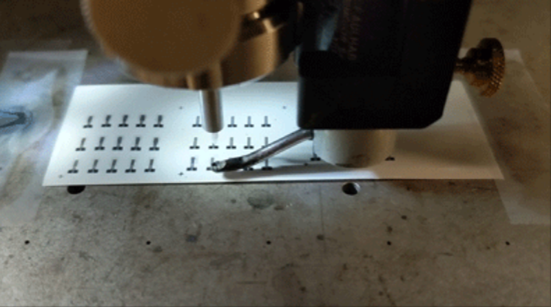
I recognise the deposition method, mist maker to atomise ink then through air guided focus nozzle, I played around with mist makers many moons ago, many potential uses, ideas are one thing results another.
likely an Optomec aerosol jet printer.
Well, I just imagine years, perhaps decades before we’re traveling in the far riches of the universe, and we need to make a transistor to make an algorithm to find the next wormhole. Ha ha ha I’m feeling white and nerdy peace out.