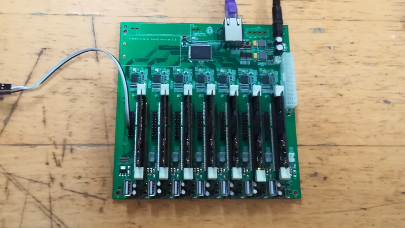
The Pine64 folks have given us so many tasty pieces of hardware over the last few years, but it’s fair to say that their products are for experimenters rather than consumers and can thus be a little rough around the edges at times. Their Clusterboard for example is a Mini-ITX PCB which takes up to seven of their SOPINE A64 compute modules, and networks them for use as a cluster by means of an onboard Gigabit Ethernet switch. It’s a veritable powerhouse, but it has an annoying bug in that it appears reluctant to restart when told. [Eric Draken] embarked upon a quest to fix this problem, and while he got there in the end his progress makes for a long and engrossing read.
We journey through the guts of the board and along the way discover a lot about how reset signals are generated. The eventual culprit is a back-EMF generated through the reset distribution logic itself causing the low-pulled line to never quite descend into logic 0 territory once it has been pulled high, and the solution an extremely simple application of a diode. For anyone who wishes to learn about logic level detective work it’s well worth a look. Meanwhile the board itself with its 28 ARM cores appears to have plenty of potential. It’s even a board we’ve mentioned before, in a personal supercomputer project.


Pro tip: do not use 1A Schottky diodes for isolating primary cells. The reverse current through the diodes can be quite large, typically exceeding the maximum charging current for the cell (which may be significantly less than 1uA (depending on the cell)). One of the example schematics on that page used a CR2032, which isn’t a large cell and won’t handle reverse current.
To pass any reasonable safety test (e.g. UL), you’ll need something to limit maximum discharge current (a resistor) and at least two things (e.g. diodes) to prevent reverse (charging) current. The whole idea is that there will not be a fire even if some components on the board mysteriously develop shorts.
poor equipment cooling. They should build it vertically like a chimney
as for the reset, I wonder if it is possible to reset just one module or a random one?
shutdown -how_many 3 or 20% ;)
It is really good to see an article–any article– on the Pine organization; thank you very much. The Pine organization has taken quite a bit of unwarranted flack for not being a “production house”, whatever that means, nowadays. There are quite a few “production houses” which should be as professional as the Pine organization.
From Ms. List:
”…but it’s fair to say that their [Pine 64] products are for experimenters rather than consumers and can thus be a little rough around the edges at times…
Pine is VERY up-front about this, unlike a LOT of other “vendors”. From Pine’s very own web-site, in their very own words…
“…This is the Beta Edition of the PinePhone. The pre-installed Manjaro with Plasma Mobile OS, that ships with this edition of the PinePhone, is a beta software build. This effectively means that while core functionality of the PinePhone still an ongoing effort. Thus, the device cannot considered a consumer-ready product.”
….and…
“Beta Edition PinePhones are aimed solely at early adopters. More specifically, only intend for these units to find their way into the hands of users with extensive Linux experience.”
…and…
“DISCLAIMER
A small numbers of stuck or dead pixels (1-3) can be a characteristic of LCD screens. While rare, this should not be considered a defect. If you think that a minor dissatisfaction, such as a dead pixel will prompt you to file a PayPal dispute, DO NOT purchase the PinePhone. When fulfilling your purchase, please bear in mind that we are offering the PinePhone at this price as a community service to PINE64 community. Thank you.”
I, personally, read all their blogs so that I’m aware of all “warts”. I also intend to purchase the Pinephone–one of THE most secure, privacy-capable, AND Linux-OS-running phones available from anywhere or anyone–just as soon as the hardware keyboard option is released to production–and it is very close. Oh, and it’s one of THE most hackable and repairable of phones (the keyboard option is “do-able” because of six “pogo pins” built onto and into to motherboard; battery?–replaceable with a very standard Samsung 3000 mAH unit.
[From Jenny List–“Their Clusterboard for example is a Mini-ITX PCB which takes up to seven of their SOPINE A64 compute modules, and networks them for use as a cluster by means of an onboard Gigabit Ethernet switch. It’s a veritable powerhouse…”.
It is my understanding that Pine is so confident in their product that they “eat their own dog-food”, insofar as that they have built their own server–based on this hardware–on which their entire website operates. Could be wrong. Won’t be the first, or last, time…]
Thank you, Jenny.
i read the whole thing because i wanted to understand the failure itself but i find i still do not. the assumption appears to be that a 74LVT04 (quad not) which is simply used as a dual buffer somehow experiences “back EMF” and draws more than 60 mA, sending the PMIC into a bad state? i don’t understand where this current draw would come from. i thought back EMF was a property of inductors. it doesn’t seem realistic to me that the transient draw of a 74LVT04 switching its own input gate would draw current for long enough to matter, and i don’t understand why its downstream consumer would draw more than 60mA. i don’t understand.
can someone explain it to me? i’m tempted to think that the author doesn’t know any more than i do and has just found a superstitious unknown that allowed him to make a blind hack that happens to work….but my own ignorance is pretty deep.
Thank you.
I’ve got (far too many) years of hardware design under my belt, with all the requisite troubleshooting of very arcane problems which, of necessity, accompanies all those years of design effort, and hard-won experience.
I can’t put my feelings of this explanation any more (elegantly) simply than you have:
“I don’t understand.”
i believe the blog author meant back feed voltage, rather than “back emf” . the PMIC info was limited in how its outputs worked (so it could not be explained other than, the quad not, output driven high, was feeding the PMIC). the problem was that the RTC voltage dropped without the batteries. the “fix” was to route 3.3v to the battery pin.
Same here. I have 20 years of electronics design experience and I after reading most of the blogs (from about halfway to the end), I have absolutely no idea what is going on.
The author seems to miss several things, for example the logic gate’s -32 mA maximum current is the current limit in shotr circuit, not something the gate will always provide. And there is no back-EMF in those components, they cannot provide more voltage than is supplied to them (expect for switching transients due to inductances/transmission lines, but that is not the case here).
What I think I understood is that there is in effect a short circuit between two busses in this reset case, which causes some component to supply its short circuit current throught the diode, and the voltage drop of the diode prevents the reste from happening (as the I/O pin voltage goes too low). It seems like the fix is to add another diode to provide more current so that the voltage stays high, i.e. the shorted-to-ground path now limits the current and the voltage does not drop… I’m not sure if I’m correct because the schematics and the issues description is so vague, but if my understanding of the issue is correct, the fix is definitely not a correct one…
Thank you all, I’m glad I was not the only one’s completely dumbfounded by this “explanation”.
I read the entire thing, and one thing I’ll commend the author for : tenacious and somewhat systematic trouble shooting from the very top (Linux-/Uboot-space) to the very bottom (electron flow on the board lines). And also for documenting the entire adventure for your fellow geeks! :-)
I was screaming at the screen for a bit, where there seemed to be some confusion about how a SoC system reset and/or WDT is actually implemented. Some of the explaining/hypothesis seemed a bit confused. In the end, a WDT reset is generally no different from any other reset source – it asserts an internal signal line to the on-die reset controller logic that will in turn assert the SoC reset tree(s), typically with some pulse-stretching and synchronization etc (which is the purpose of the reset controller). Exactly like it would if triggered from any other reset source.
In any case, this wasn’t really the point anyway – eventually it was concluded that the WDT was working as intended.
The subsequent mumbling about “back-EMF” seemed more misplaced, almost kind of mumbo-jumbo-ish. I concluded that it was probably just confused terminology, maybe it should be read as “back-feeding”. That feels more likely in this context.
In the end, could still not wrap my head around exactly what was going on, without digging further into detailed schematics and datasheets for the PMIC and so on.
And that much I really don’t care enough anyway.
But I do appreciate the story & opportunity to learn something from OPs efforts.
Also interesting to consider how one would probably have approached the investigation myself. More to the EE side, I would likely have started at the other end with hooking a probe to the reset-line. Maybe could’ve seen it sooner – but on the other hand would’ve been dumbstruck when it comes to Linux and device trees etc.
Hi, I’m the OP. In school we used to say EMF or PD for voltage is all. Back voltage feed works too.
The reset is supposed to be purely mechanical like on the smaller Pine board. Connecting one mechanical switch to 7 computers is a challenge. Pine did a good job solving this, but the PWROK from the PMIC (with no simulatable schematics) drops and never comes back fully on WDT reset. How does it go from 3.3V to 2.25V on WDT? That’s a big voltage drop, and PWROK isn’t variable. Some resistor fell on the board? I concluded there is back feed voltage (I wrote back EMF) from the inverters (the gates are chained, BTW) and the AAs compensate for that.
Then I realized the AAs won’t last long from current measurements, so they must be fighting against something – that back feed voltage perhaps.
I cannot edit the hardware, so I found a simple source of 3.3V NOT from the battery nor PMIC and called it a day.
I did consult with an electrical engineer and we were stopped by not knowing the internals of the PMIC. HTH.
– Eric Draken
Also having read this very detailed and generall useful review of the key factors involved I was also not 100% clear how the problem comes about and how the solution solves it.
But having experienced the same problem when scaling this product we looked at trying the same solution.
What we did find when eventually manage to reproduce the problem we found that the difference between one module rebooting or not when using the carrier board reset pin header seemed to be an issue with the SOC and not the PMIC. The reset lines held high by the PMIC but the reset line goes directly to the SOC, in the case where the reboot works the MCU appears to tell the PMIC (presumably via SPI connection) to power blib the DC supply (and change the voltage after boot) and you see the module Led go off/on as a result. However the case where it doesn’t work there is no change in LEDs and the PMIC doesn’t seem to do anything.
Ideally these modules would involve the PMIC in the reset process and not the SOC, which is usually not something you want to depend on for the reset to complete.