Research projects have a funny way of getting blown out of proportion by the non-experts, over-promising the often relatively small success that the dedicated folks doing the science have managed to eke out. Scaling-up cost-effectively is one of the biggest killers for commercializing research, which is why recent developments in creating carbon nanotube transistors have us hopeful.
Currently, most cutting-edge processes use FETs (Field Effect Transistors). As they’ve gotten smaller, we’ve added fins and other tricks to get around the fact that things get weird when they’re small. The industry is looking to move to GAAFETs (Gate All Around FET) as Intel and Samsung have declared their 3 nm processes (or equivalent) will use the new type of gate. As transistors have shrunk, the “off-state” leakage current has grown. GAAFETs are multi-gate devices, allowing better control of that leakage, among other things.
As usual, we’re already looking at what is past 3 nm towards 2 nm, and the concern is that GAAFET won’t scale past 3 nm. Carbon Nanotubes are an up-and-coming technology as they offer a few critical advantages. They conduct heat exceptionally well, exhibit higher transconductance, and conduct large amounts of power. In addition, they show higher electron mobility than conventional MOSFETs and often outperform them with less power even while being at larger sizes. This is all to say that they’re an awesome piece of tech with a few caveats.
The gotchas are mainly related to production and reliability. The current process for growing nanotubes produces a few tubes: metallic and semiconducting. For transistors, you want to use the latter rather than the former, and getting an accurately uniform mix of tubes is tricky when they’re only 1 nm wide. Additionally, once you have a uniform, high-quality tube mixture, how do you get the tubes where you want them? Each transistor will use several tubes so a single wafer uses several trillion tubes. Even at fractions of fractions of pennies, a trillion of something adds up quickly. There have been some attempts at growing the tubes on-chip, but ALD (Atomic Layer Deposition) doesn’t nucleate on carbon surfaces.
As we mentioned earlier, there are two reliability concerns. First, carbon nanotubes of this size degrade in the atmosphere, some early ICs only lasting a few weeks before a critical channel broke. Second, multi-channel transistors (where multiple tubes are used per transistor) last longer because of redundant connections.
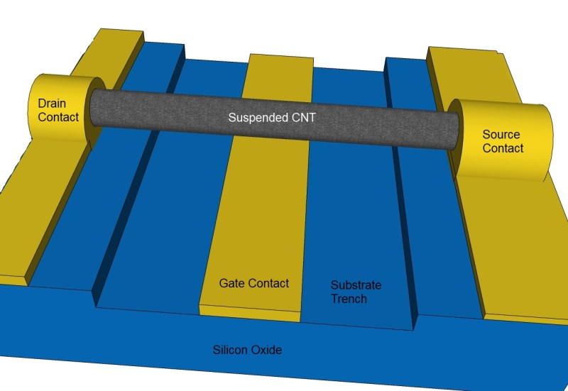
Most players are investigating the space: IBM, Darpa, TSMC, Stanford, MIT, Intel, Nantero, and dozens of others. Right there are dozens of different designs: wraparound, sheathed, suspended, top gated, and bottom gated, with no clear consensus on which is better.
This isn’t the first time we’ve talked about carbon nanotubes in transistors and hopefully, it won’t be the last. Perhaps CNTFETs (Carbon NanoTube transistors) will be used in specific spaces such as memory or low-power high-performance applications.
[Image courtesy of Wikipedia]


I see all this talk about great things Carbon can do (Graphene, carbon nano tubes, etc) but (like so many advancements in technology) it never seems to leave the lab and get turned into real world products.
Is it a case of not figuring out how to make all this new technology at a low enough price and in big enough quantities? Are there vested interests who want to hold back the new technology for some reason?
These technologies get a lot of fanfare when they’re published and then apparently vanish, but they get integrated into production processes *all the time*. We just see them as the continual incremental improvements in battery life and cpu power and device size.
I don’t understand where’s all that progress? What’s the difference between my 2012 Nexus 7 tablet and some new fancy thing from Samsung. They both do POP3 to get e-mails and they both can be utilized for basic web browsing experience.
Are… Are you actually comparing software functionality to hardware advancements?
Everything has to start somewhere, and a lot of technology experiments turn into something real. Pretty much everything, no, EVERYTHING we take for granted in our modern life has gone through this phase of development.
The giant needs to be built first, before you can stand on it’s shoulders. :)
it’s neither. the reason you hear about these advancements is because the body that invented and publicized it is interested in funding from venture capitalists.
Bingo!
(But all the above is true too — everything starts somewhere. But historically, it was with a lot less fanfare.)
It takes time. There are many, many very hard problems to solve. I got into graduate school near the end of the burst of research activity on GaN. At the time just growing sufficiently good material, even on a research scale, was a huge challenge. Then figuring out how to make n-type material, then p-type material, then basic devices and on and on. Consequently there were no real applications but lots of ‘promising for xyz’ language and a whole lot of interesting work. After many of those problems were solved a lot of the semiconductor researchers moved on to more interesting materials, but the work didn’t stop and went more into industrial R&D. Now about 30 years later we’re seeing GaN become commonplace in LEDs and power electronics etc. It just takes time and a lot of work by a lot of people.
The current hot material is Ga2O3. That might be viable in another 30 years and will be very useful if we can get it to work. But as before, we have to solve all the new problems that material hands us before we can make anything you’d get at $electronicssupplier.
I would worry about the big interconnect connect issue before making faster transistors. As you shrink the dimensions, the tracks gets thinner and their RC delay gets really bad. No matter how fast your transistors gets when you shrinks down, eventually that RC delay becomes the bottleneck.
Instead of focusing on CNT transistors, may be should look into CNT as the interconnect?
If only there were some way that people could work on more than one thing at the same time…
I kinda also wonder where’s CVD diamond semiconductors. People have been looking into that for about 20 years.
“For transistors, you want to use the latter rather than the forming, and getting an accurately uniform mix of tubes is tricky when they’re only 1nm wide”
Forming=former
Thanks! Fixed.
“Research projects have a funny way of getting blown out of proportion by the non-experts, over-promising the often relatively small success that the dedicated folks doing the science have managed to eke out.”
University press offices do this for a living, press writers use it as grist for the mill, and often sponsors of the research use it for very profitable marketing purposes. Nutrition and other dodgy “alternative” medical methods are a prime example, but the downside is the constant erosion of already marginal overall public trust in science – writ large in the age of COVID.
Just how small can any semiconductor be before it’s too small? Silicon atom is 0.2nm so 3nm is 15 atoms across.
Nothing in the 3nm process node is 3nm big. Those numbers have no relation to reality anymore and are purely marketing terms. The real feature sizes are much, much larger.
So, we’ve come full circle to tube-based technology again? ;)
(Unfortunately, Brits — who call vacuum tubes ‘valves’ — won’t get the joke.)