As great as cameras that operate in the visual light spectrum are, they omit a lot of the information that can be gleaned from other wavelengths. There is also the minor issue that visibility is often impacted, such as when it’s raining, or foggy. When this happens, applications such as self-driving cars which rely on this, have a major issue. Through the use of sensors that are sensitive to other wavelengths, we can however avoid many of these issues.
Short-wave infrared radiation (SWIR) is roughly the part of the electromagnetic spectrum between 1.4 μm – 3 μm, or 100 THz – 214 THz. This places it between visible light and microwaves, and above long-wave IR at 20 THz – 37 THz. LWIR is what thermal cameras use, with LWIR also emitted by warm objects, such as the human body.
SWIR is largely unaffected by water in the atmosphere, while also passing through materials that are opaque to visible light. This allowing SWIR to be used for the analysis and inspection of everything from PCBs and fruit to works of art to capture details that are otherwise invisible or very hard to see.
Unfortunately, much like thermal camera sensors, SWIR sensors are rather expensive. Or they were, until quite recently, with the emergence of quantum-dot-based sensors that significantly decrease the costs of these sensors.
Capturing Short Waves
The sensors that allows us to capture infrared radiation in general consist of a rectangular array of pixels, called a focal-plane array (FPA), also known as a staring array. This is similar to the FPAs used with other wavelengths, such as the CMOS (APS) and CCD sensors used with visible light. These FPAs are usually made of silicon, as silicon-based sensors are sensitive in the visible and part of the near-infrared spectrum.

For wavelengths beyond near infrared, more exotic materials and processes are generally required. The material for an SWIR sensor needs not only to be sensitive in that wavelength, but also to have sufficient electron mobility so that a charge can be transferred rapidly and efficiently enough to be of use in a sensor. This is where, at the moment, gallium indium arsenide (GaInAs) is most popular. (Also interchangeably referred to as InGaAs in scientific literature.)
GaInAs was first reported to have been successfully grown on an InP substrate by Duchemin et al. (1981) in 1980 using metalorganic chemical vapor deposition, which today is still the primary method of creating GaInAs sensor structures. After the vapor deposition phase, these GaInAs dies are meticulously bonded to a silicon-based interface, making it a relatively slow, labor-intensive and thus expensive process.
Which is not to say that it’s impossible to bump the price tag up even further. When the NIR sensors for the James Webb Space Telescope were developed, it was found that GaInAs sensors were too noisy and with high dark current. This led to the use of HgCdTe (mercury cadmium telluride) instead, with each sensor grown and assembled similarly to a GaInAs sensor, just with an astronomical price tag of around a quarter million US dollars each.
This points out a weakness of GaInAs-based sensors: in order to reduce the noise in the signal from thermal radiation, they are generally cooled down using a cryogenic cooler or similar solution. This adds significantly to the cost and complexity of operating these sensors.
The main take-away from this is that it demonstrates that there are multiple materials one can select and tune to a specific part of the electromagnetic spectrum. Which one works depends hereby on one’s requirements, as well as budget. As amazing as SWIR sensors would be to use with e.g. industrial production lines for QA and autonomous or driving-assisted cars to get around visual limitations in less than ideal weather, GaInAs-based sensors at thousands of dollars a piece are far too expensive to use in such applications.
The Right Trade-Offs
It would seem fairly obvious that for generic, affordable SWIR sensors we don’t need to match the exact sensitivity and speed requirements of a GaInAs-based sensor, as long as the trade-offs in terms of capture speed and sensitivity match the budgetary gains. This is why lead sulfide (PbS) based colloidal quantum dots (CQDs) have received significant attention, as these promise acceptable photosensitivity in the SWIR spectrum courtesy of the ability of QDs to be tuned rather precisely to the target spectrum.
A major issue with PbS CQDs is their long-term stabilization (passivation), with Kwon et al. (2020) reporting in Nano Convergence on the addition of cadmium sulfide (CdS) to stabilize PbS QDs for use as SWIR sensors. The resulting CQDs successfully operated for over 182 hours. The major advantage of CQDs like these over GaInAs-based sensors is that they are significantly easier and faster to synthesize, while also simplifying the integration into a functional sensor.
Instead of a vapor deposition step, the QDs are produced in a similar fashion as the QDs used in certain display technologies, with the QDs synthesized using solutions and equipment found in any well-equipped chemistry laboratory – as also described in detail by Kwon et al. – after which the resulting solution can be applied as a thin-film coating on the target substrate.
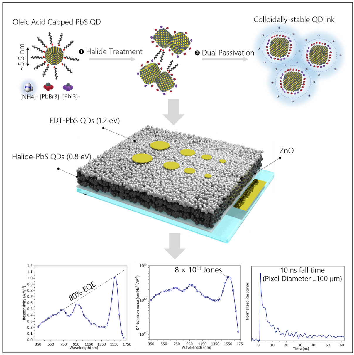
Also recently, Vafaie et al. (2020, PDF) from the University of Toronto described PbS CQDs using high-level bromine passivation, creating SWIR QDs that have not only an external quantum efficiency (EQE) of 80% at 1,550 nm (comparable to GaInAs), but also a 10 ns response time. They reported 12 hours of stable, continuous operation under ambient air.
Mind The Production Gap
Before an amazing new technology can escape from the laboratory and find its way into factories, a production process that lends itself well to mass-production has to be developed. As noted, this is where a technology like GaInAs never made it past small-scale production, but PbS CQD-based SWIR sensors appear to be doing much better.
At this point SWIR Vision Systems, Emberion, ST Microelectronics, as well as Imec have presented products using these sensors, or prototype SWIR sensors based on PbS CQDs. In January of 2022 it was announced that Hitachi Astemo as an automotive supplier will be evaluating Israeli TriEye’s Raven SWIR sensors. Being early days, it is clear that for at least a while these SWIR sensors will remain out of reach of the average hobbyist and small-scale manufacturer.
According to Imec, they expect that their SWIR sensors will ‘one day’ be manufactured for as little as €10 to €100. Compared to existing GaInAs-based solutions this would be amazing value, and put it within reach of even hobbyists once released onto the general market. This may lead one to wonder just what it is that cheap SWIR sensors would be useful for.
Inspect, Analyze, Navigate
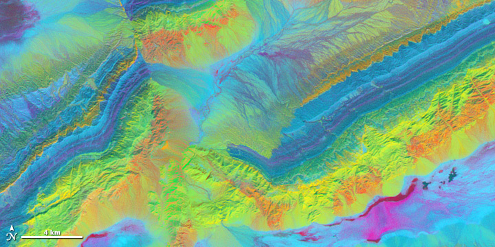
SWIR is extremely useful for contributing details that the visual part of the spectrum cannot provide, such as the mineral content in geological formations, which is essential information for NASA’s Earth Observatory project obtained using its satellites. Yet the same could be done by e.g. geologists, whether on the ground or via airplane or drone to assist surveys.
Under SWIR illumination it is also easy to see e.g. bruising in fruit, sketches hidden below the paint on a canvas, and the amount of fluid or powder left in containers that are otherwise opaque. Similarly, it is possible to see through much of PCBs and silicon, making it useful for (automated) inspections to add to existing inspection workflows.
Because SWIR is not seen by the human eye and yet reflected much like visible light, it can be used for navigation. Unlike visible light cameras, or even regular IR cameras on drones, SWIR cameras are unaffected by even the heaviest fog and rain. This is also an extremely useful property for security and wild-life cameras.
With for how many decades SWIR imaging has essentially been out of reach of the average person, it might take some time for the advantages offered to become fully obvious. Even so, when we consider the regular use that thermal cameras find today by hobbyists and professionals alike, it’s not hard to imagine SWIR cameras finding even more uses, as an alternative to both night vision (‘IR’) cameras and as an invaluable analysis tool, whether it’s sorting fruit or analyzing mineral samples.
Hopefully before long we will see CQD-based SWIR sensors become generally available. Having the current generation see use in automotive and similar markets will likely help significantly with driving down the manufacturing costs. Until then it’s still a waiting game, even as we should see these new sensors appearing in more and more devices around us.
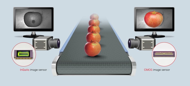
[Heading image: As apples travel down the conveyor belt, they are scanned using InGaAs and CMOS cameras. The InGaAs camera will show defects beginning to form under the skin that a human eye cannot see; the CMOS camera will show visible defects. (Credit: Hamamatsu)]


This reminds me of the first time I took the filters of of a webcam and realized that coca-cola was transparent in certain wavelengths.
As is Guinness. Surprised the heck out of me.
Someone should check on ‘Moxie’
Way back when digital cameras first arrived, they had no IR filters. This meant that photographs in certain conditions (sunlight) the IR would wash out the photo, cause havoc with image processing based on intensity, and so on.
Some people pointed out that wet bathing suits were transparent in IR, and people then took the cameras to the beach to see nude people, and (if reports are to be believed) nude children.
The result was that all new cameras have an IR filter. It’s a piece of yellow-looking glass in front of the sensor, and if you’re careful you can disassemble the camera, remove the filter, and replace it with normal glass (per the OP above).
I found that with the filter removed, the fabric fronts of my stereo speakers are virtually invisible.
If you want to explore your world in different IR wavelengths, note that you can purchase LEDs in various wavelengths pretty cheaply. It’s not hard to make a ring light around your camera of a specific IR wavelength, and take photos in the dark using the (otherwise invisible) illumination.
(I had a client who asked me to make a 3-way light source in UV/VIS/IR for this exact purpose.)
Also, diode/transistor sensors and wavelength filters of specific frequencies are easy to come by, and these can be scanned across the visual field. Scanning can be done with a laser galvo, since most IR will reflect off of a mirror.
I’ve often wondered if a projector can be reversed into a scanning sensor in this way. Place the sensor at the position of the xenon lamp and use the LCD arrays to scan the sensor across the field of view. IOW, make the LCD opaque except for a small opening, then scan the position of the opening across and down the LCD while reading the sensor output.
The IR filters on cameras do not filter all wavelengths of IR — the wavelength used in remote controls is not filtered. Don’t believe me? Point any remote control at your celphone camera and watch the IR LEDs light up when you press the buttons.
UV-IR cut filters have a finite optical density in the filtered ranges. A typical value is 3 O.D. (optical density, log10(It/I0), so a 10^3-fold reduction of IR intensity, where the quantum efficiency of Si sensors also rises towards ~1000 nm).
It’s no secret, but also not a great way to use IR for anything practical. In fact, Hoya R72 and Hoya RM90 filters are popular in photography and used with cameras that have the IR cut filter still in place. Even in bright daylight you’re then looking at exposure times of 2-30 sec.
UV Vis IR projects are great – you can matrix LEDs to get a reasonable mix for imaging, but if you’re trying to calibrate it all for spectroscopy your work is cut out for you because you’re fighting the peak/notches in the phosphor of the LED emitters and the response of the camera. Not fun at all, but there are projects out there that have done pretty well – search “webcam led uv vis ir spectroscopy”.
Look up Hadamard imaging. That is absolutely a thing. DLP/DMD devices work great for it.
They have all has IR cut filters, some just less useful than others. In fact the one in some of the early Leica cameras were so bad leica ended up sending everyone external IR cut filters to install on the lenses. With bad IR cut filters you can have focus issues because the ir light will be out of focus when you are in focus at shorter wavelengths.
Usually the IR cut filter will have a reddish reflection. If it’s yellow it may be that it is bonded to an anti-moire filter which often has a yellow hue to it.
I remember a lot of drama about a certain sony camcorder that unintentionally had this ‘feature’ built into a ‘night mode’ when digital camcorders where all the rage, pretty sure that thing is still considered illegal in a lot of countries hehe.
SWIR imaging is often advertised for security / defense applications, as unlike thermal IR it can provide high resolution video at good video frame rates.
Unlike hunting and related activities, I’d have died to actually see what happened when SpaceX’ SN11 launch was reduced to a yellow glow in the fog, followed by pieces of scrap falling out of the gray soup that was the sky on that day. At 10-20k€ entry-level price tags, SWIR cameras seem to have been out of reach, or out of scope of many popular youtubers covering such events.
Thermal IR has high res and frame rates. I have older thermal IR cameras microbolometer and stirling cooled sensor that are 640×480 at 60Hz. Of course these are ITAR restricted. FLIR also have 1080 thermal cameras available. Of course these cameras are rather expensive. The binoculars that the cooled camera was integrated in sold for about $70k.
It can see though opaque objects, but could be used for navigation?
Next week’s headline: “Tesla’s collision avoidance is “rubbish” on bin-day as car ignores all wheelie bins on street”
Underlining the point that (sometimes) we only want to see through that which we also might move through.
Guinness is a surprising one. I don’t drink, so I’ve not encountered that one yet. Fascinating though. It makes me want to test other things now.
You can still do this with an old cell phone. I have a samsung s9 that is in a tight case. I glued a 62mm filter mount to the case that completely covered the lens and now I can switch between ir filters to look at different wave lengths or just take normal photos. This still works because while cell phones do have ir filters they are thin and crappy. I like the s9 in particular for this purpose because of its age and location of the camera in the center of the phone. It is way easier to attach the mount.
“old phone” heh – I thought you were gonna say “A Nokia 3210” or somesuch…
The linked announcements mostly focus on camera sensors. Are there more affordable low-res/single-pixel options? (Similar to how a good thermal camera still isn’t cheap, but IR thermometer parts are?)
SWIR can “cut through” fog and rain? Is there such a thing as an SWIR Laser? If there is that could be used for short range laser communication that isn’t whipped out by a slight mist, might be something to look at.
Yes, SWIR is used for landing cameras for planes.
A few things pop out at me here, tired as I am from an all-night shift, so forgive me if anything is too crazy “off” here:
1. Pb, Cd, Hg, Br, etc…if you live in the EU, it seems unlikely you’ll be able to get these as a hobbyist.
2. IR cam tech is regulated pretty tightly by ITAR (and some lesser stuff like EAR in the USA). FWIW, mid-band (5uM I think but not looking) is the band used for heat-seeking missles & the like. For Near-IR (up to 2 or microns?) I don’t know. I do specifically remember (because I looked it up a few years ago when the rules changed) that, for the US Govt at least, EAR applies to un-cooled cameras but full ITAR applies if you even apply a Peltier cooler (technically).
3. Elephant in the room: how bad is cooling needed? I guess up to 2 or 3uM you still don’t need it? Can’t remember. Check Goes-16 (East) vs Goes-17 (West, with its broken loop heat pipe) for how bad cooled versus un-cooled can be on different bands.
1. Really? You can’t buy lead weights for fishing? I would expect cadmium and mercury to be the most difficult to find, as they are potentially much more harmful even in solid form—er, elementally pure form, I guess, since mercury is a liquid.
My understanding was that the EU’s hazardous materials regulations applied mostly to the manufacture of products to be sold, so I would imagine you could still buy from industrial suppliers. Here in the US, cadmium goes for about $3/kg right now, mercury is relatively easy to come by, bromine is a controlled substance but can e pretty easily extracted from hardware-store chemicals.
I would think that the process to even attempt manufacturing anything with this process would be much more difficult than getting the materials, even if you had to smuggle them in using questionable methods. The cost and need for a controlled environment in any kind of vapor deposition like this is so much more prohibitive than access to the (relatively cheap, if hazardous) materials.
I’m interested to know what the process is for a private citizen to obtain “banned” elements for scientific/industrial use.
I did quite a lot of work on swir camera technologies in the 2000’s. The InGas sensors we’re good enough, but didn’t get any less noisy below -120C. Quantum dots were a thing back then too. Also had a LWIR camera from the 70’s, it mechanically scanned a 7*1 lead based detector array, and mechanically scanned the 7 outputs to red LEDs, the scanner produced a 70 lone display. LWIR lenses made it remarkably useful.