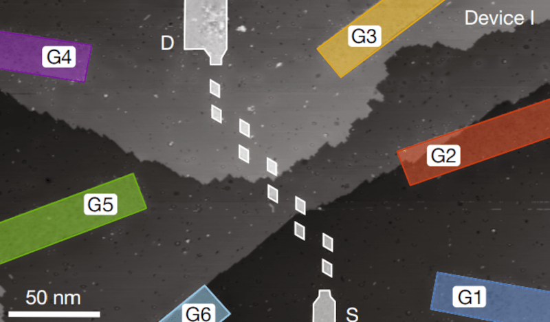
Researchers at the University of New South Wales and a startup company, Silicon Quantum Computing, published results of their quantum dot experiments. The circuits use up to 10 carbon-based quantum dots on a silicon substrate. Metal gates control the flow of electrons. The paper appears in Nature and you can download the full paper from there.
What’s new about this is that the dots are precisely arranged to simulate an organic compound, polyacetylene. This allowed researchers to model the actual molecule. Simulating molecules is important in the study of exotic matter phases, such as superconductivity. The interaction of particles inside, for example, a crystalline structure is difficult to simulate using conventional methods. By building a model using quantum techniques on the same scale and with the same topology as the molecule in question, simulation is simplified.
The SSH (Su-Schreffer-Heeger) model describes a single electron moving along a one-dimensional lattice with staggered tunnel couplings. At least, that’s what the paper says and we have to believe it. Creating such a model for simple systems has been feasible, but for a “many body” problem, conventional computing just isn’t up to the task. Currently, the 10 dot model is right at the limit of what a conventional computer can simulate reasonably. The team plans to build a 20 dot circuit that would allow for unique simulations not feasible with classic computing tech.
The dots are made with a scanning tunneling microscope and there is a Goldilocks effect regarding the size of the dots. If they are too small, the energy levels are overwhelmed by phosphorous donors. Too large, and capacitive coupling between dots makes the system unstable.
We’ll admit, the science in the paper is pretty dense. But the Methods section outlines what it takes to create something like this. You’ll need silicon, high-temperature ovens, and the ability to handle exotic gasses and perform lithography. Pretty much an IC fab in your basement. However, we did wonder if anyone homebrewing chips had ever tried STM lithography like this as an alternative to optical lithography. Seems like it might be possible.
We can’t help with some of the more exotic gear, but if you want to build an STM, it has been done. While you can make quantum dots in your kitchen, we don’t think they are going to work the same.


What about the actual molecular level?
https://github.com/iaddis/metalnes
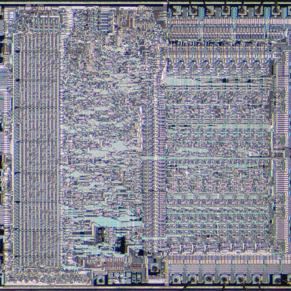
Transistor level NES-001 simulation.
Though technically you could work on the actual molecules at a large enough scale that it actually does what this group is doing. Except they are currently at about at a single molecule in the above post. Pretty sure the NES has more than a few molecules in total.
There is also GateBoy, featured here.
https://hackaday.com/2021/09/07/gateboy-is-a-game-boy-emulated-at-gate-level/
Of course there is http://www.visual6502.org/.
Has not been updated but Visual NES
https://github.com/SourMesen/VisualNes
This is a C++/C# port of the Visual 2C02 and the Visual 2A03 by Quietust (http://www.qmtpro.com/~nes/chipimages/visual2c02/). It combines both simulators into a single simulation and allows the simulation to run NES roms (albeit at roughly 1/1000th of the speed of a real NES).
“moving along a one-dimensional lattice”
This makes my brain hurt. How is a one-dimensional lattice possible? A lattice, as far as I understand it, by its very definition would require at least 2 dimensions, wouldn’t it?
Lattice does have rather dry formal definitions as a type of partially ordered set. It could be more similar to those definitions?
Lattice is a bit of a poor word to use here. But a 1D lattice is simply a chain. It’s 1D because it can be fully described by one variable: the distance along the chain.
My brain corrects it to 1 dimension of a lattice, unless otherwise informed. Meaning they intend to simulate atom spacing in a lattice, and not let everything jumble up into what shape it felt like, if you just left 10 atoms to their own devices.