When making a PCB informative and self-documenting, there’s often just not enough space to silkscreen all the labels you want, and slowly but surely, you collect a set of tricks: using different through-hole pad shapes to denote ground or power pins, standardized pinouts for connectors, your own signal name shortening notations, and so on.
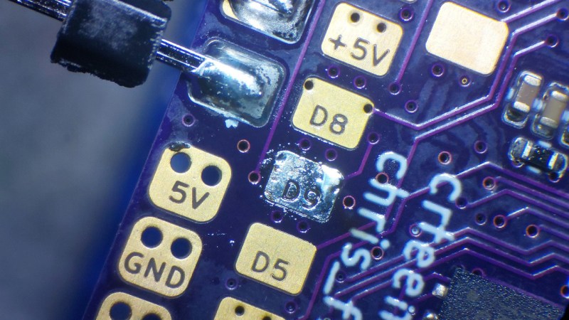
What if you have some large-ish signal pads on your board, and having the signal names on silkscreen just isn’t good enough? In this case, here’s a new trick for your toolkit: [Christoph] from [MakerProbe] shows us how he puts text directly inside the copper pads.
What you need is a set of Gerber files and a Python script. Technically, this ought to work with any PCB EDA, with [Christoph] using KiCad. You need to put the to-be-subtracted signal names on their very own layer, export Gerber files without features like aperture macros, then run the script. You’ll get a new copper layer as a result, it’s that simple. We also get a set of tips on what kinds of pads suit best and how to prepare them — and fancy-looking real-life examples. You get higher resolution than for on-silkscreen text, solderability isn’t impacted, and the labels are even visible after desoldering wires from the pads. What’s not to like?
Over on Twitter, [Makerprobe] have been doing things like 0201 tombstoning and BGA yield research – we say they’re worth a follow if you’d like to see someone pushing PCB boundaries! Innovative PCB design methods and tricks have a special spot in our hearts, what’s with things like this Tux-emblazoned desktop motherboard that’s also a guide on PCB aesthetics, and there’s a whole lot more you can do to make your PCBs pretty while preserving and even improving functionality. From turning rigid PCBs flexible to hiding components inside a PCB stack, there’s plenty of opportunities that we are yet to extract out of PCB world, and it’s lovely to see one more technique we can make use of.
Tutorial: Text-in-pad with gerber_combinehttps://t.co/5eFwHXIzcR@hackadayio @oshpark @AislerHQ #electronics #kicad pic.twitter.com/c50js9Q5BH
— Makerprobe (@makerprobe) March 24, 2023


I remember I saw marking flags look like resisitors, but just a wire with PVC labels soldered into PCB.
Trapping contaminants under joints, that’s not to like.
While an interesting idea at first blush, I’m pretty sure any of the contract manufacturers I’ve dealt with would instantly reject this.
It’s not the brightest idea to solder over etched areas because you can expect the gases trapped under the solder tent above the etched area to expand and contract with each heat cycle of the soldered component. In addition – how the flux is supposed to be cleaned from those covered surfaces?
It would be fine if no solder was applied to those areas with etched labels – such as if they were to be used for example as capacitive buttons or a front plate for some instrument, though.
Also: those unfilled/unplugged vias in the solder pads… hopefully they’re not blind, but still…
don’t you lose the labeling once you solder on to it? so whats the point?
Photo in the article (and article text) sure the label as legible when covered with solder.
And with the connecting wire… Maybe not
“component blocks label” is a problem for regular old silkscreen, too. Particularly since the footprint is often the only nearby empty space.
How can we see the pad marks when they are soldered?
Terrible idea.
I guess it looks cool to some people, but I don’t see how that would out way the risks involved. Trapped gasses and residual flux, as mentioned above, could easily be a problem. I’ve also seen a lot of pads being pulled up and damaged during repair – or even production for that matter. So I’m curious to see how well this type of labeled pad can hold up to repair work compared to a perfectly solid pad.
Y’all feel free to implement labels in your pads, but if I’m out of space for the silkscreen, I’m just going to accept the fact that I ran out of room and should have used larger pcb dimensions.
If you are surface mounting a part to the “top”, but the pad is through hole, text could go on the “bottom” side. Labels are still visible after soldering, but need to stop solder drainage through the via.
Pre-filling the via with resin is one technique to prevent this.
As a person working in a PCB fab, don’t do this. On top of reasons stated before in the comments, the width of the text is very weak thin strip of photoresist that has a habit of floating off or drifting before it gets the galvanized negative image from tin 😁
Yours and the other comments is what always keeps me coming back to this site. So much to learn!
sounds like you’d have the same problem with small fiducials though, and those wouldn’t be fair to not-recommend.
I feel this was posted on Hackaday 3 days too late? 🤷
yeah there was a delay, but, late is better than never showing a cool thing to our readers!
I think this is really cool. The biggest downside is that after you solder the component you can’t see the label. But before that it’s more clear than having the text next to the solder pads.
Lots of people talking about why this is bad. But it sounds like it’s mostly speculation from armchair-engineers. This might not be a good idea for production designs, but for personal hobby boards it looks fine to me. Actual testing will determine how bad or good it really is. I hope to see more people testing this out.
Glad to hear you’re an expert on who’s an armchair-engineer and who’s had 40 years of experience in the industry. I’ll be sure to check back with you if I have any questions.
I’m confused as to what you gain by trying to convince people to do this. The idea is very cool, but the issues pointed out in the comments are real and reasons why you shouldn’t.
Lot’s of negativity here, yet I like this from a test point only point of view. I will plate with ENIG, no solder will be used on such a pad. My boards are typically inside enclosures and it can be difficult to locate the associated silk-screen designator as well as hard to see. I think this will absorb light in the etched text and make it more readable. It will also delineate what is supposed to be a test point rather than just an exposed pad. I will ask my CM first, but I am guessing they won’t care if they are not soldering to it.