When you first start out in the PCB layout game and know just enough to be dangerous, you simply plop down a connector, run a trace or two, and call it a hack. As you learn more about the finer points of inconveniencing electrons, dipping toes into the waters of higher performance, little details like via size, count, ground plane cutouts, and all that jazz start to matter, and it’s very easy to get yourself in quite a pickle trying to decide what is needed to just exceed the specifications (or worse, how to make it ‘the best.’) Connector terminations are one of those things that get overlooked until the MHz become GHz. Luckily for us, [Rob Ruark] is on hand to give us a leg-up on how to get decent performance from edge-launch SMA connections for RF applications. These principles should also hold up for high-speed digital connections, so it’s not just an analog game.
Everything that happens to those unfortunate electrons along their travels will affect performance in a subtle way, but the higher the frequency components of a signal, the worse it gets. An SMA edge connector may be designed to present a characteristic impedance of 50Ω typically, but that is to the end of the connection pins. Once it’s soldered down, there is a discontinuity unless precautions are taken. Even the transition from the pad to the signal trace can push a system out of spec, but what about the stack-up? What about the ground plane under the pad?
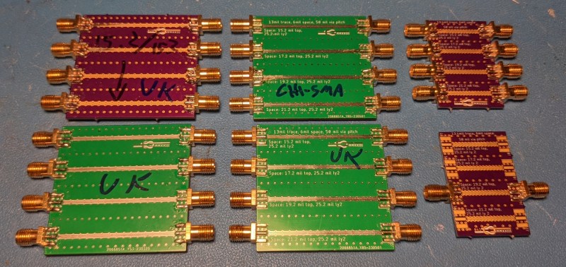
The first part of the job is to lock down your PCB process, via a specific stack-up. Every PCB house and line within it is different from the next, so it is critical to get hold of the layer arrangement, foil and dielectric thicknesses, dielectric constants, and loss tangent figures. [Rob] took a typical route, making a first stab at a footprint design supported by lots of online calculators (like these by Chemandy Electronics) and reference material. The basic structure is the usual coplanar waveguide, where the e-field is constrained by the ground plane below and leaks over the top of the trace. This resulted in a set of test coupons (small test PCBs) for two fab processes in parallel, OSHPark and JLCPCB.
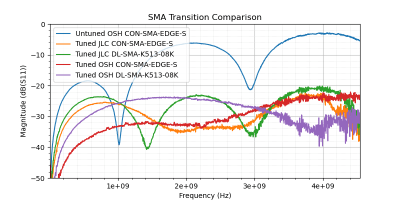
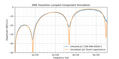
The returned PCBs were characterised using a NanoVNA V2 Plus, to get the S11 (return loss) curve up to about 4.5 GHz, confirming at about -26 dB they were already in a good position for optimisation. [Rob] also goes into some details about how to line up a QUCS simulation of a lumped transmission line model with the measured test coupon performance, which is well worth digging into.
PCB design is about functionality, but it is also about aesthetics and other factors that come out of that. Also on the subject of transmission lines, there are other kinds of transmission lines to read about.






I wish there were cheap bandpass filters for the cheap 2 meter handheld transceivers.
Depends on the power class you need to handle, efficiency, and filter design.
The main issue is there is a lot of bad designs (dubious ferrite choices in kits) that have haunted the internet for years. A modern “fixed” version of a LiteVNA-64 VNA, and QUCS… will get you 80% of the way design wise.
Mini-Circuits stuff was always premium, but the quality is arguably worth the price:
https://www.minicircuits.com/WebStore/dashboard.html?model=BPF-F150%2B
…or you may get an RSI winding your own Toroidal inductors. =)
73
VE7NTP
Thanks for the link!
I guess I am expecting too much for “cheap”.
At $70, the filter is almost twice what I paid for the HT.
Maybe that is why the mfgrs leave out the components that would clean up spurious signals.
The cloned 5W SDR modules in cheap mobiles are under $10 including delivery. The issue is the $5k fine plus a year in jail for splattering the spectrum with a clone of a clone. There are simple DIY filters that also fix up counterfeit Nagoya antennas too, but no one seems to take the time to fix cheap equipment.… hence why the UV5R were banned. ;)
Fix:
https://www.qsl.net/z33t/english_page1.html
https://www.youtube.com/watch?v=jBNcTn9BEy0
Bookmarked!
Thanks again!
Feel your pain ;-) I too collected a significant chamber of horrors of test coupons while doing a 1.8GHz design on FR4. I used QUCS & QUCS studio including the inbuilt transmission line calculator. The trick was to periodically run test coupons to determine the FR4 dk parameters to correct in the calculator. After a few runs of the loop and a lot of hours with the excellent PicoVNA I was starting to see clean 50R transitions. The next step was to build a dodgy clothes peg test interface to further work on the filter/circulator/component CPWG tapers & transitions on the board between the connectors without having to use a soldered SMA. Later, one of the usable SMA tricks that I found was to put a few spaced small circular holes in the underside gnd plane copper under the pin to reduce capacitance & hit the 50R target. C19 saw the end of the project however the next few months will see the topic revisited for a UAV project.
How did tou go about simulating multi-layer designs in QUCS / QUCS Studio?
I was mainly using them for the transmission line calc & lumped component sim along with SimSmith. Started to look at physical layout sim in Sonnet Lite & OpenEMS before the project folded. In the intervening 3 years the software has moved forward so looking forward to getting back into the puzzle ;-)
The project was using 2 layer FR4 for the RF components back then but the higher frequency on the new project will require Rogers.
Bringing back lots of memories before I went down a different career path. I fought with many RF designs to eek out every last fraction of a dB. It wasn’t just a matter of what type of material you made the board from, but what brand, and even what board house.
My favorite tool was wcalc https://wcalc.sourceforge.net/
Useful posting.
“These principles should also hold up for high-speed digital connections, so it’s not just an analog game.” is because digital signals are transmitted by analogue waveforms. The receiving circuit interprets the analogue waveforms as digital signals.
At the risk of teaching grandmothers to suck eggs, that’s true for all clock frequencies, and logic families; the highest frequency depends on the transition time, not the time interval between transitions. Even with jellybean 74LVC1Gxx gates, it is possible to have transitions 1GHz.
The only digital signals likely to be encountered are photon counting circuits and femtoamp circuits. Are there others? :)