From the consumer space it often would appear as if Intel’s CPU making history is pretty much a straight line from the 4004 to the 8080, 8088 and straight into the era of Pentiums and Cores. Yet this could not be further from the truth, with Intel having churned through many alternate architectures. One of the more successful of these was the Intel i960, which is also the topic of a recent article by [Ken Shirriff].
Remarkably, the i960 as a solid RISC (Reduced Instruction Set Computer) architecture has its roots in Intel’s ill-fated extreme CISC architecture, the iAPX 432. As [Ken] describes in his comparison between the i960 and 432, both architectures are remarkably similar in terms of their instruction set, essentially taking what it could from the 432 project and putting it into a RISC-y shape. This meant that although the i960 could be mistaken as yet another RISC CPU, as was common in the 1980s, but integrated higher-level features as well, such as additional memory protection and inter-process communication.
Although there were four versions of the i960 sold, they all used the same die, just with some parts not connected. The high-end XA version can be regarded as a 33-bit processor due to the full architecture’s features being enabled, including the entire ISA and object model. A year after the initial i960 release, the CA version would become the world’s first superscalar processor, and as a whole the i960 processor became a popular sight in the US military, also due to the way it worked well with the US-mandated use of the Ada programming language. In a way this fulfilled many of the promises the iAPX 432 had made.
Despite the successes, ultimately the i960 was axed by Intel after it had been neglected for many years in favor of the x86 architecture, until in 2007 the production of i960 processors finally ceased.
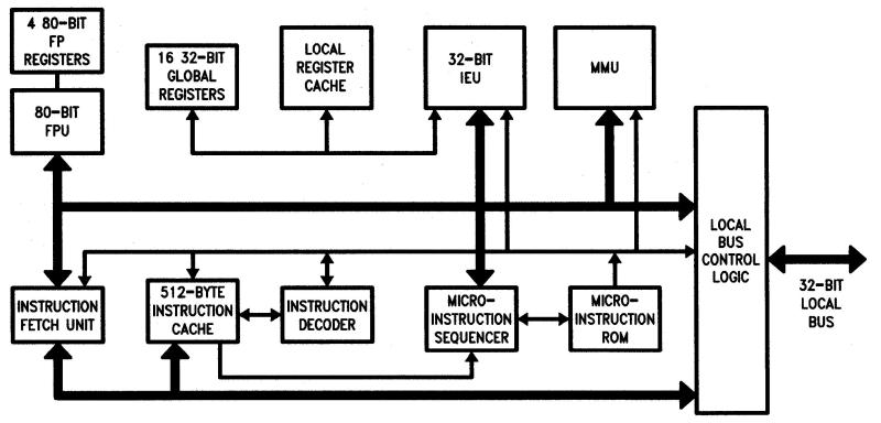
(Heading image: The microarchitecture of the i960 XA. FPU is Floating Point Unit. IEU is Instruction Execution Unit. MMU is Memory Management Unit. From the 80960 datasheet.)


Ada, what a fun language. Takes strong typing to new levels.
One noteworthy use of the Intel i960 was in the Sega Model 2 arcade machines.
Also used in many Raid Controllers, in fact if you want to source one it’s probably your best bet.
And the Namco FL board (Final Lap R, Speed Racer).
We looked into using an i960 board as part of a 3D arcade game we were developing in ’93-’94. I was responsible for the render pipeline. Have always looked back on that device fondly… Nice to read about it here!
Cool article, but inaccurate. There were several i960 based devices. All different die. I worked on all of them.
The i960cx was one of the first multiple instruction issue/ speculative execution processors. The Kx was a cheaper alternative. Sad they got killed. Huge mistake by intel.
Intel has had other flirtations with RISC besides the i980 (which was and OK processor, BTW — good for embedded work). Their x86 type processors are microcoded, though (though you’d probably never get them to admit this openly, much less tell you what/how/why) so I expect that some of that RISC technology has percolated to their main product line.
Intel had the i860 which was VLIW, and failed due to compiler issues.
You are very confused and about 2 decades out.
i860 was a RISC chip introduced in 1989.
Itanium was Intel’s VLIW chip, introduced in 2001, and which suffered from compiler issues.
I am not confused, thank you.
I know very well between the i860 and the Itanium. In fact the i860 was introduced around the time I graduated my Engineering degree.
The i860 suffered, similar to the Itanium, from requiring optimizing compilers to achieve peak performance, but these apparently did not materialize.
If you look at the i860 Programmer’s Reference Manual ( http://www.bitsavers.org/components/intel/i860/240329-002_i860_64-Bit_Microprocessor_Programmers_Reference_Feb89.pdf ), you can see that it had a Dual-Instruction mode:
…”The i860 Microprocessor can execute a floating-point and a core instruction in parallel. Such parallel execution is called dual-instruction mode. When executing in dual-instruction mode, the instruction sequence consists of 64-bit aligned instructions with a floating-point instruction in the lower 32 bits and a core instruction in the upper 32 bits.”…
That sounds like a kind of VLIW to me. The Itanium had 3 instruction in a 128-bit bundle, and the i860 had 2 instructions in a 64-bit word.
The i860 wasn’t VLIW. You’re thinking of Itanium.
i was surprised to see wikipedia says the i860 is VLIW. i downloaded an i860 “programmer’s reference manual”, and it describes a straightforward RISC ISA with 32-bit instructions and a nice uniform encoding. it definitely seems RISC to me.
there is a very stale conversation in the wikipedia talk page about the designation as VLIW. it apparently hinges on a “dual execution mode” where it fetches two 32-bit instructions at once and executes them simultaneously, with some significant limitations. it also has a “vector model” but i don’t understand a thing about it.
it seems like it is a chip with a RISC instruction set but nonetheless a lot of pointless complication. intel of the 1980s and 1990s seemed to have a distinct aversion to the principles of RISC. it is really kind of surprising to look at. seems like they had 3 different flirtations with making their own ISA to exploit RISC but in each case they added pointless complication for the purpose of guaranteeing no one would ever want to use it.
i think it’s interesting to see that something as abstract as ‘good taste’ can permeate such a large institution and have such concrete results.
The i860 was supposed to be a high end workstation CPU. Its extensive pipelining was also its downfall as it took about 2000 clock cycles to respond to an interrupt. That said it was extremely fast (once it had its pipelines filled) for its day. The fpu was optimized for 3d and matrix operations.
There were a few pc motherboards made with both an i486 and i860. You needed specially ported software apps to take advantage of the i860. I know AutoCAD was one.
The “dual instruction mode” requires two specific instruction types, one “core” (load/store/integer) and one floating point in a specific alignment in consecutive 64-bit words. Compared to the Itanium with a 128-bit bundle and three 41-bit ops, it is pretty much the same idea.
” Their x86 type processors are microcoded, though (though you’d probably never get them to admit this openly, much less tell you what/how/why)”
Given they regularly and publicly publish microcode updates, maintain a github for the updater (https://github.com/intel/Intel-Linux-Processor-Microcode-Data-Files), document it in the processor architecture SDMs, etc, the only way one could think Intel do not ‘admit’ the use of microcode is by an active refusal to look.
Unpopular truth is that x86 is a good architecture. Some things could be improved, for sure, but there are fewer of those things than people think there are, and ultimately, they didn’t really matter.
In architectural terms, the 8086 was certainly worse than the 68000 and the 80386 worse than 680×0, NS32016, MIPS, Sparc, ARM, etc.
The reasons why: few registers; idiosyncratic use of registers; arcane addressing modes; segmentation.
It was successful, because it was easy to convert from 8-bit 8080 code to the 8086 (and the 8080 was popular with business computers in the late 70s via CP/M) and most importantly, because IBM chose the 8088 for its PC.
In addition, Intel engineers put a massive amount of effort into giving post-1990s x86 processors competitive performance with RISC designs. It’s amazing what you can do with 10x the number of engineers. This in itself is an indication that the architecture is poor (though x64, designed by AMD is notably better).
We don’t have to pretend the x86 is a good architecture on top of recognising its success.
Agreed, when you delve into assembler, it’s nasty.
The only thing I’ve experienced that are worse, are Z80 and TI TMS DSP.
Funny you mentioned the Z80 as it is a supped up 8080 with an extra set of registers.
The Z80 is more frustrating to program than the 8086 or x86 successors, primarily because it’s really a dual accumulator architecture (A for 8-bit stuff and HL for 16-bit arithmetic) and it has limited addressing modes for accessing data (namely indirect register, and inefficient (IX+n), (IY+n) 8-bit access).
On the other hand it’s an 8-bit architecture that’s an extension of the 8080 and many of the architectural compromises were forced by that. Friendly 8-bit designs are difficult. The 6809 (and to an extent the 68HC11) are relatively easy to program for, because again, although it’s a dual / triple accumulator architecture (A, B or D for 16-bit access), it has a good set of addressing modes. You don’t find you need to juggle registers and it’s all fairly consistent. The 8-bit AVR MCU is quite nice to program for, it’s a good design.
When we compare 16-bit architectures, it’s best to compare them with other 16-bitters IMHO. So, we might want to compare the 8086 with the Z8000 (the Z8000 is cleaner despite having a smaller transistor budget); or the pdp-11 (the pdp-11 is far more regular, in fact very regular); or maybe compare with the 68000 which is like a 32-bit version of a pdp-11 and a well-thought out design.
And it’s best to think about the rationale for its development, namely that (a) they had a customer (not IBM) who needed a CPU with at least 128kB of addressing and high level language support so upgrading the 8080 was a fairly quick and dirty way to get there*; (b) The i432 was already failing and they needed something to plug the gap.
So, the 8086 wasn’t motivated by idealism, but expediency, whereas the 68000 was motivated by the goal of leap-frogging the emerging 16-bit processors and not bothering about compatibility with existing CPUs.
Most CPUs have an underlying objective. The 8-bit PIC for example was a Peripheral Interface Chip designed by GI to compensate for the poor IO performance of their 1600 CPU. The 6502 was motivated by the designers of the Motorola 6800 believing they could develop a much cheaper and more efficient CPU. The TMS 320C010 (its first DSP) was motivated by the desire to improve maths performance on a single CPU: they didn’t care much how hard it was to program, because they assumed that the utilisation of efficient algorithms far outweighed the development costs. And it was very efficient for its day.
The 32-bit ARM processor was motivated by the early RISC processors and the belief that a small British company (Acorn) could achieve the same kind of thing as the Western Design Centre if they made a super-simple, super-energy efficient CPU.
The 1980s Transputer was motivated by the idea of creating multi-core CPU boards about 20 years before their time. Parallel processing was built into the CPU and it’s possible to take pretty much the same parallel code and algorithms running on a single core and run them on a whole matrix of CPUs. Mind-blowing!
The 16-bit Data General NOVA minicomputer in the late 1960s had a very crude, austere design motivated by the idea of reducing costs by cramming a whole processor onto a single 38cm PCB. It’s much harder to program than an 8086 (bad), but about the same logical complexity as an 8080 (genius). The multi-function ALU and SKIP condition instructions likely influenced the ARM processor 15 years later.
*I found this out via an email from the person who designed the 8086.
heh i think this is an interesting way to put it.
i don’t think x86 is a good architecture. i960, i think, shows that it could be worse! maybe x86 is better than some possible competitors. and i think that is something worth remembering when pondering why x86 succeeded so well.
but “they didn’t really matter” seems well borne out in reality. for a while i thought the performance per watt metric was going to matter (vs ARM). but after a few generations, that turned out to look like rounding error too.
it is really remarkable how costs can be encapsulated. after intel and AMD pay the cost of ridiculous instruction decode logic, and once gcc and clang pay the cost of writing a codegen for the ridiculous register set, those costs simply disappear. i used x86 for 32 years before i knew how ridiculous it is to try to make efficient code for the x87 stack-based FPU, and in those 32 years it had already been obsoleted multiple times over by different kinds of MMX/SSE. and i never even had to notice the transition. even today, all i have to know about SSE is that a subset of it is a relatively common sense register-based FPU. its complexity just looks over-designed to me because if you really wanted to do that much parallel or looped math you’d use a GPU these days. and i don’t have any idea how GPUs work either!
And one more important thing: the ‘C’ language – hides the ugliness and renders the beauty of the code
You might want to change the title to i960 as you write in the article as I960 looks like the year 1960 to idiots like me.
Loved the i960 in the day, mainly because it had a whole boatload of interrupts, especially compared to the more arcane x86 interrupt model. It made creating high speed device drivers very easy.
It was a very good embedded chip, and if Intel did not have such a x86 fixation, could of created a nice niche in the market, instead of abandoning it to ARM
Let’s remember that Intel ran its own StrongARM/Xscale product line from 1997 to 2006. They got it from DEC in settlement of its patent infringement suit in 1997and sold it to Marvell. Arguably, they used it to replace i8/960s which were ailing by that time.
I remember helping bootstrap Linux onto the i960 dev boards waaay back when…
These were truly a beautiful chip, the last true capability architecture, and even cleaner than CHERI or ARM Morello. Stoked that Ken is looking into them!