Doing anything that requires measurements in nanometers is pretty difficult, and seems like it would require some pretty sophisticated equipment. But when the task at hand is growing oxide layers on silicon chips in preparation for making your own integrated circuits, it turns out that the old Mark 1 eyeball is all you need.
Alert readers may recall that [ProjectsInFlight] teased this process in his previous video, which covered the design and construction of a DIY tube furnace. In case you missed that, a tube furnace is basically a long, fused quartz tube wrapped in electrical heating elements and lots of insulation, which is designed to reach the very high temperatures needed when making integrated circuits. The tube furnace proved itself up to the task by creating a thin layer of silicon dioxide on a scrap of silicon wafer.
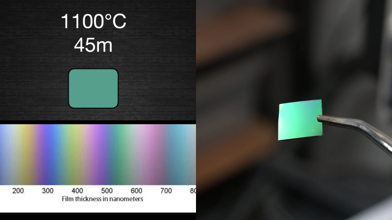
In the current work, [ProjectsInFlight] takes that initial success and builds on it. A lot of the video below is devoted to explanations of what exactly a silicon oxide layer is and why you’d need one; if you’ve never been introduced to the subject matter or your understanding is shaky, this section is actually really valuable. The actual creation of silicon oxide starts at about the 7:45 mark, with an exploration of the effect of time in the furnace on layer thickness. This is measured by the color change on the surface of the silicon as the silicon oxide layer grows. It’s a bit subjective, but with some careful measurements of time and temperature, the results are pretty predictable.
One area where [ProjectsInFlight]’s simple tube furnace design caused problems was with maintaining a proper atmosphere. As he touched on in the first video, silicon oxide formation is much quicker if water vapor is present. He used a simple steam generator — a flask of water on a hot plate — but found that his oxides weren’t forming as expected because the steam was actually condensing before even making it into the tube furnace. The solution was simple — more heat and better insulation — and he was able to reliably build oxide layers in the 350 to 400 nm range.
This looks like great work, and we’re excited to see the next steps along [ProjectsInFlight]’s road to homebrew semiconductors.


I hope he is successful in making MOSFETs before the zombie apocalypse!
There’s always that question of, how far do you think you’d get, if you were dropped back into the past and had to start from scratch.
I think I’d get eaten by a wolf, or beaten to death by the locals and then eaten by a wolf. Even if I were only dropped a hundred years in the past, and wolves went extinct in this country 500 years ago, I’d still be eaten by a wolf.
I like and respect your optimism.
I could get us up to the modern era.
I wouldn’t though, these people are retarded.
B^)
+1
I will certainly start with power source and relay logic, perhaps for UI using Nipkow disc. Now the problem is, am I able to produce relays? No I am not, it all ends with fact, I am not able to produce thin wire.
The issue that people keep forgetting is that all the manufactured stuff will still be here after the zombie apocalypse, and even after a nucleair blast. Thin wire will be ubiquitous.
Personally I find that electricity and fire will be quite easy to create. Glass too. Copper wire is out there.
But one of the first important things you would want to make is electric light. And for that you need iron, glass, and tungsten.
…AND something to create a vacuum… Or an inert gas like Argon.
Both of which are quite hard issues to fix. Producing a relay is actually quite simple compared to this problem. :)
Vacuum for carbon fiber light bulb. The Edison bulb. Argon under pressure for a tungsten bulb or you plate the inside with tungsten. Then there are carbon arc, and discharge tubes which are easier. Carbon arc needs no vacuum but does need UV blocking glass.
Wait so the oxide layer is getting pushed up from the silicon? Like the oxide on the outside is actually the first oxide that formed?
yes. Roughly. It is a little more complex as it is a diffusion process, but to a good approximation.
The real Mark 1 eyeball was nothing more than a biological photodiode! The human eyeball is like the Mark 129048932043920432 eyeball, very advanced.
1 cone, 1 nerve neuron, 1 capillary, 1 cortical neuron
Ahhh the old oxide color chart. In backend manufacturing, typically everything is controlled, so when customers would change their backside oxides, it would impact certain processes. They’d always argue nothing changed, but then you just show them light result and the fact they’ve doubled their thickness over night, and then they go….”Oh by the way, we’ve changed (blank)” haha. Also, it’s a really good method for verifying whether your spin coater is too slow/fast/time is too long/short/etc or if the table is at a weird angle(you’ll see funky patterns around the side).
more such anecdotes please !
So cool! Really looking forward for the future vids!
I hope he let the A.I. developed a chip for the: ” The answer to life, the universe and everything”, build that Chip and ask him the question: “The answer to life, the universe and everything”.
this were such a cool nerdy art project.