Making RAM At Home In Your Own Semiconductor Fab

There’s little point in setting up your own shed-based clean room for semiconductor purposes if you don’t try to do something practical with it. Something like responding to the RAMpocalypse by trying to make your own RAM, for example.

Testing the DRAM cells. (Credit: Dr. Semiconductor, YouTube)

After all, what could be so hard about etching the same repeating structures over and over? In a recent video, [Dr. Semiconductor]’s experience doing exactly this are detailed, with actual DRAM resulting at the end.

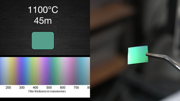
We covered the construction of the clean room shed previously, which should provide at least the basic conditions to produce semiconductors without worrying about contaminating dies. From here the process is reminiscent of etching PCBs, with a prepared surface coated with photoresist. Using UV exposure through a mask, the pattern is etched into the photoresist and from there the pattern is subsequently etched into the wafer’s surface.

With the patterns formed, the next step is doping of the silicon in order to create the active structures, i.e. the transistors and capacitors. Doping can be done in a variety of ways, with ion implantation being the industry standard method, but a bit too expensive and bulky for a shed fab. Instead a spin-on-glass method was used. After this the remaining functional structures can be built up.

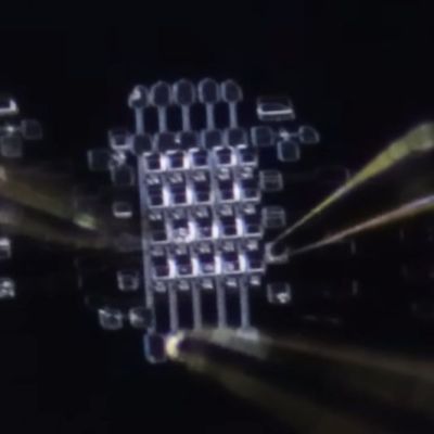
If anyone was expecting to see a DDR5 DRAM die pop out at the end, they’re bound to be disappointed. The target here was to create a 5×4 array of DRAM cells, for a dizzying 20 bits. Still, the fact that it’s possible to DIY DRAM like this at home is already pretty awesome, with clearly plenty of room to push it towards and past fabrication nodes of the 1990s and beyond.

Although the produced DRAM cells have fairly leaky capacitors, they’re good enough for their purpose, and the plan is to scale up to a large DRAM array from here. Whether the DRAM control logic will also be implemented in hardware like this remains to be seen, but the video’s ending makes it clear that the goal is to attach it to a PC somehow.

Continue reading “Making RAM At Home In Your Own Semiconductor Fab”

Lab-grown diamonds in 'cake' form -- before they are processed and polished.

Why Diamond Transistors Are So Hard To Make

Many things about diamonds seem eternal, including the many engineering problems related to making them work as a silicon replacement in semiconductor technology. Yet much like a diamond exposed to a stream of oxygen-rich air and a roughly 750°C heat source, time will eventually erase all of them. As detailed in a recent [Asianometry] video, over the decades the challenges with creating diamond wafers and finding the right way to dope pure diamond have been slowly solved, even if some challenges still remain today.

Diamond is basically the exact opposite as silicon when it comes to suitability as a semiconductor material, with a large bandgap (5.5 eV vs the 1.2 of silicon), and excellent thermal conductivity characteristics. This means that diamond transistors are very reliable, albeit harder to switch, and heat produced during switching is rapidly carried away instead of risking a meltdown as with silicon semiconductors.

Unlike silicon, however, diamond is much harder to turn into wafers as you cannot simply melt graphite and draw perfectly crystallized diamond out of said molten puddle. The journey of getting to the state-of-the art soon-to-be-4″ wafers grown on iridium alongside the current mosaic method is a good indication of the complete pain in the neck that just this challenge already is.

Continue reading “Why Diamond Transistors Are So Hard To Make”

I, Integrated Circuit

In 1958, the American free-market economist Leonard E Read published his famous essay I, Pencil, in which he made his point about the interconnected nature of free market economics by following everything, and we mean Everything, that went into the manufacture of the humble writing instrument.

I thought about the essay last week when I wrote a piece about a new Chinese microcontroller with an integrated driver for small motors, because a commenter asked me why I was featuring a non-American part. As a Brit I remarked that it would look a bit silly were I were to only feature parts made in dear old Blighty — yes, we do still make some semiconductors! — and it made more sense to feature cool parts wherever I found them. But it left me musing about the nature of semiconductors, and whether it’s possible for any of them to truly only come from one country. So here follows a much more functional I, Chip than Read’s original, trying to work out just where your integrated circuit really comes from. It almost certainly takes great liberties with the details of the processes involved, but the countries of manufacture and extraction are accurate. Continue reading “I, Integrated Circuit”

Crystal structure of a monolayer of transition metal dichalcogenide.(Credit: 3113Ian, Wikimedia)

Transition-Metal Dichalcogenides: Super-Conducting, Super-Capacitor Semiconductors

Transition-metal dichalcogenides (TMDs) are the subject of an emerging field in semiconductor research, with these materials offering a range of useful properties that include not only semiconductor applications, but also in superconducting material research and in supercapacitors. A recent number of papers have been published on these latter two applications, with [Rui] et al. demonstrating superconductivity in (InSe2)xNbSe2. The superconducting transition occurred at 11.6 K with ambient pressure.

Two review papers on transition metal sulfide TMDs as supercapacitor electrodes were also recently published by [Mohammad Shariq] et al. and [Can Zhang] et al. showing it to be a highly promising material owing to strong redox properties. As usual there are plenty of challenges to bring something like TMDs from the laboratory to a production line, but TMDs (really TMD monolayers) have already seen structures like field effect transistors (FETs) made with them, and used in sensing applications.

TMDs consist of a transition-metal (M, e.g. molybdenum, tungsten) and a chalcogen atom (X, e.g. sulfur) in a monolayer with two X atoms (yellow in the above image) encapsulating a single M atom (black). Much like with other monolayers like graphene, molybdenene and goldene, it is this configuration that gives rise to unexpected properties. In the case of TMDs, some have a direct band gap, making them very suitable for transistors and perhaps most interestingly also for directly growing 3D semiconductor structures.

Heading image: Crystal structure of a monolayer of transition metal dichalcogenide.(Credit: 3113Ian, Wikimedia)

Stacking Solar Cells Is A Neat Trick To Maximise Efficiency

Solar power is already cheap and effective, and it’s taking on a larger role in supplying energy needs all over the world. The thing about humanity, though, is that we always want more! Too much, you say? It’s never enough!

The problem is that the sun only outputs so much energy per unit of area on Earth, and solar cells can only be so efficient thanks to some fundamental physical limits. However, there’s a way to get around that—with the magic of tandem solar cells!

Continue reading “Stacking Solar Cells Is A Neat Trick To Maximise Efficiency”

Growing Oxides On Silicon On The Road To DIY Semiconductors

Doing anything that requires measurements in nanometers is pretty difficult, and seems like it would require some pretty sophisticated equipment. But when the task at hand is growing oxide layers on silicon chips in preparation for making your own integrated circuits, it turns out that the old Mark 1 eyeball is all you need.

Alert readers may recall that [ProjectsInFlight] teased this process in his previous video, which covered the design and construction of a DIY tube furnace. In case you missed that, a tube furnace is basically a long, fused quartz tube wrapped in electrical heating elements and lots of insulation, which is designed to reach the very high temperatures needed when making integrated circuits. The tube furnace proved itself up to the task by creating a thin layer of silicon dioxide on a scrap of silicon wafer. Continue reading “Growing Oxides On Silicon On The Road To DIY Semiconductors”

Gordon Moore, 1929 — 2023

The news emerged yesterday that Gordon Moore, semiconductor pioneer, one of the founders of both Fairchild Semiconductor and Intel, and the originator of the famous Moore’s Law, has died. His continuing influence over all aspects of the technology which makes our hardware world cannot be overstated, and his legacy will remain with us for many decades to come.

A member of the so-called “Traitorous Eight” who left Shockley Semiconductor in 1957 to form Fairchild Semiconductor, he and his cohort laid the seeds for what became Silicon Valley and the numerous companies, technologies, and products which have flowed from that. His name is probably most familiar to us through “Moore’s Law,” the rate of semiconductor development he first postulated in 1965 and revisited a decade later, that establishes a doubling of integrated circuit component density every two years. It’s a law that has seemed near its end multiple times over the decades since, but successive advancements in semiconductor fabrication technology have arrived in time to maintain it. Whether it will continue to hold from the early 2020s onwards remains a hotly contested topic, but we’re guessing its days aren’t quite over yet.

Perhaps Silicon Valley doesn’t hold the place in might once have in the world of semiconductors, as Uber-for-cats app startups vie for attention and other semiconductor design hubs worldwide steal its thunder. But it’s difficult to find a piece of electronic technology, whether it was designed in Mountain View, Cambridge, Shenzhen, or wherever, that doesn’t have Gordon Moore and the rest of those Fairchild founders in its DNA somewhere. Our world is richer for their work, and that’s what we’ll remember Gordon Moore for.

You can read our thoughts on Moore’s famous law. If you ever wondered how Silicon Valley became the place for electronics, the story is probably much older than you think.