How many terminals does a MOSFET have? Trick question since most have three leads, even though there are really four connections to the underlying device. It isn’t a conspiracy, though and [Aaron Lanterman] talks about how MOSFETs really work and why thinking of them as three-terminal devices can lead you astray in a recent video that you can watch below.
Like many people, [Aaron] points out the parallel between a triode vacuum tube and a MOSFET. That’s not surprising, since a solid-state tube was exactly what they were looking for when they developed the FET. Since tubes and FETs are both voltage controllers, it is easy to think of the gate as the grid, the source as the cathode, and the drain as the plate. But, [Aaron] shows this isn’t really a very accurate picture.
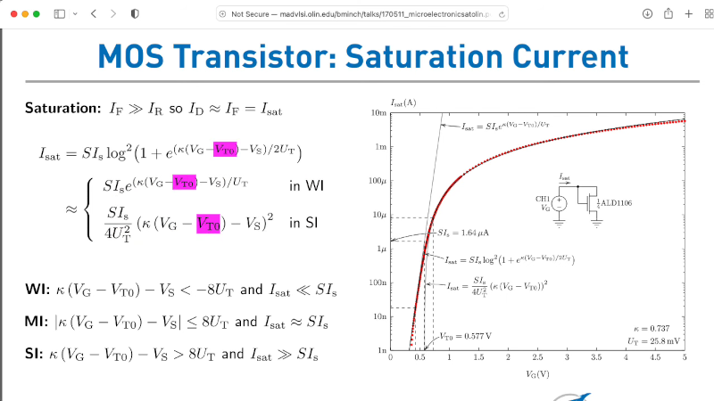
The fourth terminal of the MOSFET is the “bulk” or substrate. In a package, we typically see that tied to the source, and that actually defines the source since, on a four-terminal MOSFET, the source and drain are interchangeable as long as the device is symmetrically built. If you are working with three-terminal devices, this means that Vgs — the voltage from gate to source — is meaningful. But with a four-terminal device — or one constructed on a die — you must realize that the gate voltage will work differently than the source voltage since there is a built-in offset from the bulk terminal.
If you only use packaged MOSFETs, this difference is probably only a curiosity. However, it is good to understand how things really work and, too, designing custom ICs is becoming more accessible every day. Understanding the details of components can lead to interesting designs. Like using a MOSFET as both a heater and a temperature sensor.


Four terminal discrete MOSFETs do exist. I have had several 2N4351 FETs sitting around for a while now. I might even find a use for them sometime.
I’ve used some of them in the past, mostly 3N2xx parts to build RF preamps and mixers for receivers I built for fun.
They have become harder to find lately, but NOS parts from eastern Europe can be a cheap substitute. Also, a dual gate MOSFET can be made out of two jFETs as shown in this pic.
https://www.researchgate.net/profile/Vahid-Kouhdaragh/publication/311455931/figure/fig6/AS:469206106939397@1488878861300/Dual-MOSFET-Gate-Schematic-14.png
There is a nifty application in Horowitz “The art of electronics 2nd edition page 224 ”
Integrator reset.
“you must realize that the gate voltage will reach differently from the source voltage since there is a built-in offset from the bulk terminal.”
Instead of “reach”, did you mean “react”?
I’m a bit confused by that sentence.
One of the newest technologies is the gate-all-around MOSFET. In these devices, the substrate does not contact the channel (because the gate is all around the channel). Except for parasitic effects, the substrate does not affect the current through the channel.
Also, there are silicon-on-insulator MOSFETS, including silicon-on-saphire, that have no electrically meaningful substrate.
Good point! I wonder how LVS device extraction would be handled for GAA or CFET devices. Still 4-terminal?
I posted this in reply to the video and will re-post here:
I respectfully disagree. Vgs is still a useful approximation even for IC design since the bulk terminal is usually not changing too much. You do have to be careful about Vth varying with bulk voltage and account for that when doing the initial design (this can be almost entirely avoided with SOI processes, which also allow more freedom to adjust circuit parameters using the back gate). Additionally, the square law approximation is very back of the envelope for modern processes anyway, short channel effects like mobility degradation and velocity saturation are generally more important in my opinion.
Other people have mentioned that most modern devices are FinFET devices where the square law model breaks down even further.
It’s only a big lie if you’re doing IC design. If you’re using MOSFETs in three-terminal packages, the source and gate are internally connected, and you can use the simplified formula.
Yep, click bait headline… as if this is news after 60 yrs…not.
It’s also a poor and irresponsible use of the phrase “the big lie” which has real historical relevance as well as relevance to current events.
Ouch! I’m sure that Al was unaware of the resonance there. Will change.
So, if you have access to one of these devices, can you bias the “Bulk” terminal so as to change the threshold voltage, and independently change the biasing of the input gate voltage? Electrically this could be very useful in designing analog amplifiers, and could provide a method of biasing the input voltage to correctly work in an output amplifier stage.