Ordering a PCB? Two of them? Three? Five? For about eight years now, I’ve been regularly ordering large numbers of different PCBs, and, naturally, have developed a toolkit to make things smoother. One trick is PCB panelization, and you should really know about it.
You might’ve encountered PCB panels already. Perhaps, if you order PCBA at a fab, you will get your board returned in a whole new form-factor, with rails on the sides that you have to snap off before your PCB is usable. Those rails are used so that your PCBs are easier to handle during assembly, but that’s far from the only reason why you would make a panel.
If you need multiple pieces of a PCB, your fab may say that building 50 pcs is classified as “large batch” and that takes longer than 30 days, which delays your entire PCB order. I’ve been there, five years ago, running out of time right before Chinese New Year. The fix was simple – I made a 2×2 panel and ordered that in quantity of 10-15. Panelization might be a little more expensive, or maybe even cheaper, but, most importantly, it will be faster.
In a few hours’ time, I sat down, figured out that KiCad has built-in features for panelization, and ordered panels instead of separate PCBs. Thanks to that, I made the Chinese New Year deadline that year and could successfully restock my store, letting me earn a fair bit of money instead of keeping a popular product out-of-stock – ultimately, helping my family stay up on rent that month.
Panelization lets you hack around many PCB ordering and assembly limitations, and I’ve only gotten started – there’s way way more! For now, let’s sort out panelizing multiples of the same PCB. As long as your boards are using KiCad (or KiCad-converted from Eagle/EasyEDA/Altium/gerbers), there’s no better software than KiKit.
KiKit Simply Rules
 KiKit is a KiCad plugin by [Jan Mrazek], and it’s had a ton of work put into it to make it a one-stop shop for KiCad panelization. Once installed, KiKit lets you do panelization from inside KiCad, with a nice GUI that lets you define all sorts of parameters. Install it and go wild. KiKit is a little tricky to install and there’s some slightly uncomfortable behaviour – in other words, just like the majority of the software we use, but it brings you massive benefits for some possible initial pain.
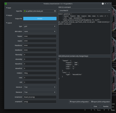
Open an empty board by opening pcbnew (PCB Editor) standalone, then, in the top toolbar, press the KiKit button on the right. Pick a board in “Input”, click “Output” and enter something like panel.kicad_pcb, set rows and cols to something like 2 and 3, hspace and vspace to 2mm, set Cuts=>type to mousebites, and press Panelize in the right bottom corner.
This is the most basic panel you could do, and if you ever have had to draw such a panel manually, you will notice that this just saved you a ton of work. This panel has no fiducials, no outer frame, no V-cuts, but all of these are just a couple dropdowns and digit fields away. Want to order a large number of PCBs? This is how you do it, and there’s a good few uses for this. One of them for me used to be decreasing prices at JLCPCB, but as they ramped prices up over the years, this benefit has faded – another PCB fabs might still give lower prices for panels for you, however, so watch out. There’s other uses that remain true, too.
Panels So Nice To Handle
I designed a large-ish capacitive touch panel a couple years ago, a pandemic-related project that would help mark your attendance of something like a hackerspace. It used a custom touch controller and giant electrodes: 2 cm x 2 cm PCBs with rounded edges. I wanted to have a dozen kits of them, which would’ve led to a batch size of 200 and increased production time that’d delay my entire order.
Instead of ordering 200 of a single PCB, I made 4×4 panels. They were way cheaper, quick to manufacture, and way easier to manage once received. I wanted to mail them out to some hackerspaces, and the panels also helped – instead of counting out 16 of them and then having them rattle around in an envelope, I could take a single panel and throw it into the package. A cherry on top is that your PCB’s recipient gets the satisfying task of splitting a V-cut panel into separate PCBs, too.
Here’s another example from the PCB design above. It’s a shim for a Linux-powered Raspberry Pi that lets you program SPI flash chips with the standard “SPI flash” pinout – SOIC-8, SOIC-8W, and DFN. With this shim, you don’t need to carefully match jumper wires – just desolder the chip in question, solder it onto the shim aided by elongated pads, then plug the shim onto a Pi header; it will hold onto the Pi GPIO header pins and make electrical contact thanks to staggered holes.
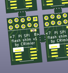 This shim proved to be an indispensable tool for quickly dumping and reflashing SPI ROM chips, and I’ve been mailing these out to people as “throw in envelope” gifts. I’ve now run out, need to order more, and I see that I feel bad mailing just one of these – they’re incredibly cheap, easy to use, and very nice to have around. With panelization, I can order multiple and send out panels of a dozen at a time, they’ll remain incredibly cheap, and I can throw them into envelopes without any rattling action – plus, the recipients get to break away the tabs.
There’s more, of course – once you scale up a project of yours, you can easily do manufacturing with these, and, again, save a fair bit of money!
The Fab Wanted It, So I Improvised
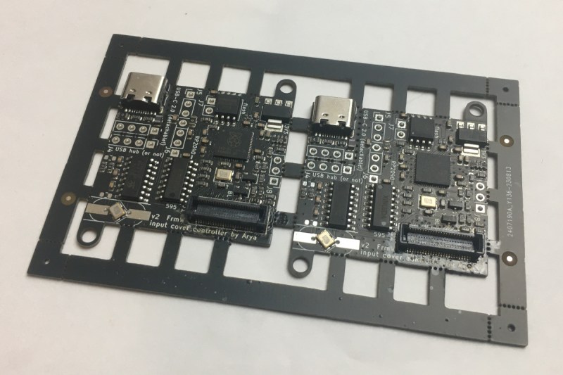
For manufacturing, it’s common that your board needs a panel around it; specifically, a thin PCB frame with the board held inside by mousebite, with perhaps even on-frame fiducials for assembly positioning. This makes your possibly-unorthodox-shape board into a panel that an assembly house workers and their machinery can easily handle. Sometimes you can have the fab handle the panel stuff, but some assembly houses will want you to mail your files already prepared, rail added and all. KiKit makes such panels a breeze, as you might guess.
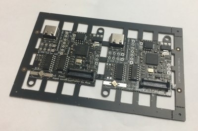
panel.json for this specific panelOnce again, you can save a fair bit of money if you make such a panel. Take JLCPCB’s “economic” tier PCB assembly service – it’s notably cheaper than “standard”, but it has limitations on what you can do. For instance, you have to pick from a list of allowed PCB thicknesses and soldermask colours. I needed two-layer 1 mm thick black PCBs, but I wanted like 50 of them where economic assembly would only allow 30. On this board, having to use “standard” assembly would be a significant price jump with no benefit at all.
Instead, I made the PCB into 1 x 2 panels with KiKit and ordered 30 panels – each panel counts as a PCB for PCBA purposes. This let me order 60 pcs of an assembled PCB significantly cheaper, at the cost of some depaneling once the boards arrive, which, again, that’s just a fun thing to do. JLCPCB might clamp down on this and force you to use more expensive assembly, but, for now, you can easily fab 150 pcs of a small PCB while still keeping within economic assembly tier.
Once you’ve defined the frame for the PCB, KiKit will have some JSON that defines your panel’s parameters. Don’t just close the PCB editor you’ve been KiKit’ing in! Exporting KiKit’s JSON is vital, unless you want to re-configure the parameters every time you need to regenerate the panel; I usually save it as panel.json in the folder where the board file is. In fact, there should really be an autosave option – anyone up to do a pull request?
Naturally, with KiKit boards, you can easily export pick and place data – the end result is just a KiCad board, you can even edit it afterwards. I typically use a fab-aimed plugin when ordering PCBA, but you can also just export .pos and .csv BOM files the same way you would from any other KiCad PCB.
Tips And Tricks
V-cuts are pretty clean to handle: you just snap the boards apart. Mousebites are perhaps less so because they leave jagged edges on the PCB. Watch out here – using sandpaper on the edges is not the greatest idea, with this dust being both carcinogenic (it’s fiberglass dust, remember!) and abrasive. The resulting dust is going to go everywhere, it’s irritating in a literal sense, and you might even end up having to wash it off your PCBs. Instead, try using a box cutter with those snap-off blade sections, sliding it against the board outline – it should be able to cut off the jagged edges, leaving no dust, just slices of mousebite remains.
As a footnote, here’s a tactic I want to try out – using V-Cuts for making castellated modules on the cheap. I don’t want to pay a significantly higher price for a special castellated process, but I still want to PBCA like 100 pcs of a cool small module so I can throw it into postal envelopes and put it on my products; also, V-Cuts feels like you’d get nicer plated edges than milled. I don’t know if a fab would accept it, but this article says it’d be okay to do and such holes can work as inter-board interconnects. I’m out to try this trick out soon, and will report back!
We’ve panelized a single PCB today – which is cool and helpful, but there are even more exciting options. Next time, I’m going to show you how to save even more money and maybe make assembly even quicker, as well as save a fair bit on SMT stencils – stay tuned!

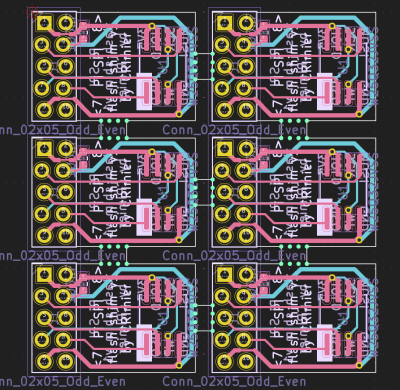


remember, you are paying them to throw away the material between the boards, do you really need gaps that big?
If I had to guess, there is a standard size of rectangle that they are targeting. So I imagine that it wouldn’t be any cheaper if it was smaller.
I think the question was more in line with…
Is there another sheet size that lets you tesselate your boards with less gaps?
If the next sheet size is 25% larger, but you can fit 4 boards on it instead of 2, you are making less waste.
You have a lot of extra web material on those panels… you could easily drop 1/3rd of those tabs (middle tab of every group of three) and still be plenty stiff for automated PnP. The reduction in tabs will also allow for reduced pressure necessary for depanelization (assuming you’re stuck snapping panels rather than cutting/nibbling).
There’s also no reason why the semi-circular tab with the hole in it can’t extend into the panel frame as there are no components on it. You may not get an even 100mil route around both boards without making the frame too thin in those areas, but you could certainly reduce the wasted material.
yea I forget our rules as its been a min since I did penalization I think production asks for 10mm from the edge to a component and 7mm for a fiducial. I have taken them all the way out to the very edge many times before with features like that
back in my day, panellization was the only option. Three PCBs (no more, no less) at $33 apiece was an incredible bargain that brought professionally-made PCBs into the realm of possibility for anyone besides big corporations. 3x 10in x 15in made for a lot of boards! And it was quite a skill to design them to fit together like puzzle pieces, and include prototype space whereever possible. a patch of 4×16 0.1in spaced holes here and there made for some excellent flexibility multipurposing single-purpose boards… Nevermind fixing design mistakes without running another order. A single row of 0.1in through-plated holes between boards makes them snappable on the edge of a table, but also, if needed, can be cut on either side with a bandsaw to add a header to a board…
The list goes on. Then cheap-fabs came out. Heh. So much for all those skills!
Do you have a source for the assertion that FR4 dust is carcinogenic?
Hi, cancer is not the correct name, fiberglass can cause fibrosis in the lungs just like asbestos. https://doh.wa.gov/community-and-environment/air-quality/indoor-air/fiberglass
Pretty much all tiny hard sharp dust is when you breathe it.
Even if it isn’t, it can(will eventually ) still cause major health problems.
(Silicosis, emphizima, etc)
That is why breathing protection is MANDATORY.
Not the usual Dave. Just sayin.
Tell me about it.
B^)
Hi there, Ren
Ex-electronics assembly tech here: mousebites are designed to be cut off with a large nibbler. The jaw needs to be wide enough to cut in one movement.
Usually this looked like a router table, with a pneumatic nibbler jaw in place of the router bit, and operated with a foot pedal.
“… this article says it’d be okay to do and such holes can work as inter-board interconnects.”
I suspect you meant to link “this article”? I’m interested in that, as a multiple-board stackup is a solution to a particular layout issue I’m having with a Framework 16 keyboard module. I’ve done the “poor man’s castellation” with a milled edge and it does work but leaves your copper pretty chewed up. Curious to know if a v-cut will end up cleaner.
oh right, thank you, fixed; it’s this article, for reference!
A few notes:
(I used to run a circuit card factory). DISCLAIMER- what worked for us for “low volume” (10-100/mo) might not work for these ultra low volume needs.
1) Your best bet is to understand your vendor’s standard panel size and build your panel as something divisible into that. Effectively, the extra boards you can cram into that panel are”free” (almost). The economics are stunning.
2) V-cuts are fine, but the strain on depanelizing these has broken many a chip cap. Bad if your units get into the field and start blowing up because of internal fractures. If you have SMT on your assembly, I recommend the mouse bites, dog bones or equivalent. V cuts can work— we never liked them.
3. Just go ahead and put fiducials on your panel, even if you think you won’t need them. They’re easy to add, and you will. I personally would also add a tooling hole in the panel- always the same size, always the same place.
Hope this info is useful
KiKat really should have been named KitKat, because you break pieces off a larger piece.
Sorry, “KiKit”.
Too bad panellised of various designs is not allowed and counted as separate designs and thus not cheaper :(
good news, the next article will talk about that in depth ^_^
waiting patiently…
Tuesday?
Yes I did this by hand to make 4 prototype different designs on one panel.
But if KitKat (!) can do that it would save a lot of fiddling about.
Oooh! Keyboards, perhaps?
Cheap PCBs need to be below 10cm x 10cm (4 x 4 inch). If you take inspiration from the “Butterfly” design of the 701 Thinkpad, could you make a keyboard using the SAME PCB?
For ortholinear, you simply place 2 or 3, side by side. A conventional staggered layout would mean flipping one board upside down.
I see it let’s you select type like “grid” what other options are there? I have some hexagon shaped pcbs I’d like to panelize but they’d need to have equal spacing and correct offsets in alternating rows like a honeycomb. Is this possible?
We need an extension to fill in a plate with usefull small circuits.
Instead of empty “arms” like on the panel of two, we should use usefull pcb.
even just 0.1in protoboard would be extremely useful.
That might be considered a ‘seperate design’ and they might charge you for that, although Arya is hinting at an upcoming post that will address this (see above). Cant wait!
They didn’t charge by surface ?
Many cheap PCB houses (e.g. JLCPCB, PCBway, etc) will already detect ‘on the sly’ panelisation like this and either reject the board outright, or add the surcharge for panelised designs and treat it as a large batch anyway. Either they’re doing this with automated design tools when they receive your gerbers, or during master panlisation where your attempt at panelisation is very obvious.
I never understood such rules… it’s a cheap tactic to charge more. I have run into that issue multiple times in years past. One design was several boards that WERE identical, but the intent was to provide a small (single) panel with multiple PCBs to the customer… think of a DIY kit where the customer stuffs components using different BOMS to achieve different functionality, and the frame served double-duty as a structural element in the final build. The fab house didn’t understand that last part, so they were solely focused on the multiple copies of the same PCB design within the frame. I had to practically scream at the sales guy to get that one through.
A second design had different silk on each board. Same argument, the electrical CAD looked the same, so you’re trying to cheat the system. Less screaming involved, but it was still exasperating and time-consuming.
How have I typically solved it? I connect a ground trace on an inner layer between all of the PCBs (or a pour, depending upon design). After separation, a 6-mil slip of copper at the edge of a board is all that shows, and that usually affects nothing. From a CAM perspective, the entire panelized PCB looks like a single electrical net for ground, so there’s no reason to kick it out.
you’re confusing single-board panels with multi-board panels! JLC doesn’t have that significant of a surcharge for “same design” panels, they’re an accounted-for case with their own button and different from “Different designs” buttons. In particular, “treat it as a large batch anyway” is false for single-board panels, I know, because that’s how I get them.
ok can someone help me out? my ignorance is profound.
when you panelize, you take your like 2″x2″ design and copy it over again to fill up some like 10″x10″ build area that all their machinery can do efficiently? with the appropriate borders and padding and what-not, right?
if you order just a single copy of your 2″x2″ design, how is that different? isn’t their big innovation in the past 20 years some software that lets them automatically panelize every design that comes in off the street? don’t they put it on a panel with however many copies of other customer stuff?
or is it just that the pick and place is more efficient if there’s only one kind of board, with a less diverse parts list??
i’m trying to understand what this article means in the actual physical production. or is it just a hack to get around a pricing metric?
When I do a batch of something for a personal project I always panelize. its much easier to handle 10 boards of 10 rather than 100 individual units, I generally don’t care about making it easier for them, that’s their problem, its for me … the guy who has to apply solder paste and stuff smt components, and reflow 100 boards
When using V-cuts be sure that the layer gets into the gerber exports.
I have put them in user layers before…recently I was advised to put them in the “edge cut” layer and to clearly mark them as vcut on each line.
I like the vcut on small boards (adapter boards and such) but more often than not I end up forgetting the labels for the vcut. With JLCPCB there is very little cleanup needed. To be safe you can always sand the edges with wet emery cloth or similar. Always good to not breath that dust though.
If you are milling your boards there is a PCB cutting fluid that precisebits.com sells which limits the dust.
In my case I also use the “stencil8” method for my paste jig. This requires that a few of the mechanical holes in the board also translate to the paste layer. This is another area where clear marking in the gerbers is important. Either they will question them and delay your order…or forget them entirely.