
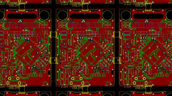
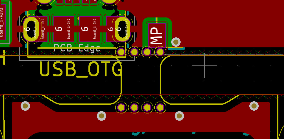
We might consider PCB panels as simply an intermediate step towards getting your PCBs manufactured on the scale of hundreds. This is due to, typically, an inability to run traces beyond your board – and most panel generators don’t give you the option, either. However, if you go for hand-crafted panels or modify a KiKit-created panel, you can easily add extra elements – for instance, why not add vias in the V-Cut path to preserve electrical connectivity between your boards?
[Adam Gulyas] went out and tried just that, and it’s a wonderfully viable method. He shows us how to calculate the via size to be just right given V-Cut and drilling tolerances, and then demonstrates design of an example board with discrete component LED blinkers you can power off a coin cell. The panel gets sent off to be manufactured and assembled, but don’t break the boards apart just yet — connect power to the two through-hole testpoints on the frame, and watch your panel light up all at once.
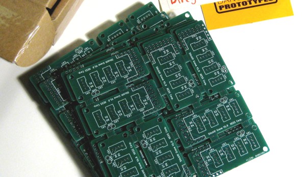
It’s a flashy demonstration – even more so once you put light-diffusing spheres on top of the domes. You could always do such a trick with mousebites, but you risk having the tracks tear off the board, and, V-Cuts are no doubt the cleanest way to panelize – no edge cleaning is required after breaking the boards apart. Want to learn about panel design? We’ve written and featured multiple guides for you over the years.


 Great minds think alike, and this guide is following hot on the heels of [Brian Benchoff’s]


