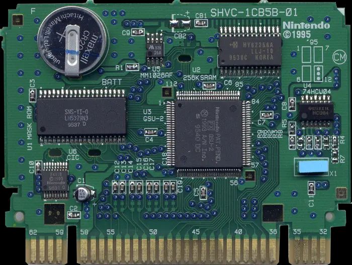
Despite being effectively sold as a toy in the 1990s, the Super Nintendo Entertainment System (SNES) was pretty bleeding-edge as far its computing chops were concerned. This was especially apparent with its cartridges, such as in this excellent summary article by [Fabien Sanglard].
In addition to the mask ROM that stored the game data and (optionally) battery-backed SRAM to store save data, a wide range of enhancement processors existed that upgraded the base SNES system with additional processors for more CPU performance, enhanced graphics and so on. Imagine sticking a game cartridge in a PlayStation 4 today that boosted CPU speed by 5x and gave it a much better GPU, this was the world of SNES games.
On the other side of the video game cartridges was the video output system, which seems easy enough in today’s world of digital HDMI and DisplayPort output. In the 90s video output did however mean NTSC and SECAM/PAL, which means playing nice with frequencies, different resolutions (lines) and squeezing as much as possible into a single frame in a way that works with the game console’s rendering pipeline. As a result of this the PAL version of Super Mario World has a larger vertical resolution than the NTSC version (240 vs 224 lines), even if it’s still squashed into the same 4:3 format. For the physical video output side, European gamers were spoiled with an AV connector to (RGB) SCART output, while the rest of the world dealt with some variety of RF composite or S-video.
Although the SNES’s successor in the form of the N64 would not take cartridges to the same extremes, it was this flexible architecture that gave the SNES such an amazing game library.


I yearn for a future where sillicon fabs are so ubiquitous and common that unity and other game engines have an “export to HDL” option along with the usual “export for windows” or whatever
Imagine never having to buy a console and only having to buy an SD card sized state machine which can run one game, and only one game at 1000Hz framerate.
Then add a “Turbo” microswitch that instead slows it down to a more managable 60MHz for computers that don’t correctly adhere to the timing.
Not sure most can afford a monitor with a 60 MHz framerate =P
I wonder what’s going on with the blue over the vias on that PCB – it’s not just the green silkscreen over gold is it (?). And the elongated holes with traces going to them eg. above and left of “U2 256k SRAM” but there are a couple of others.
But dots every 5 pins on the big ICs – good idea!
The elongated holes are probably for programming or debugging. Mill the traces away when the board is ready for shipping ?
The elongates holes likely had some kind of test pin formation which was used for testing/debugging purposes. It was milled after the first few prototypes or after programming.
The blue stuff over the vias is likely a kind of resin soldermask to insulate any exposed copper since the vias are done after etching and applying the normal green soldermask
Per discussion I read elsewhere, the blue covers on the vias are “tented”, of a specific sort. Paraphrasing: Probably wave soldering, dry film soldermask over/in addition to a liquid soldermask, to keep the liquid soldermask out of the via.
Elongated holes are for electroplating – everything must be shorted together for plating, and then they mill out the shorts.
What are those dots every 5 pins for?
To make it easier to count pins to find the pin you want to probe. I shall be using this idea from now on.
And anyone else get an urge to “fix” C7, to the right of the big square chip U3? :-D
I didn’t, until some internet rando pointed it out and triggered me. Thanks for that.
Now what am I supposed to do? Download the image and fire up GIMP?
;-)
You can do the same on a new 3DS. It uses a multiplexed cartridge
Throw a cpld, fpga, and it even has spi iirc so even a mcu, then you can just make a docking station like a switch
New 3ds xl has the same kind of hardware as an android tablet
And it’s cartridge protocol should be fast enough to use a DSP and ram expansion (like a slower cache)
Someone did that with snes too
Throw fpga on snes
Get hardware ray tracing that superfx cant even dream of
https://youtu.be/VeFF344NbZ4?si=BoYxYtO4oRcG6zhr
You can see that it could actually compete with a 32bit playstation 1
Add another 16bit CPU, clocked by ray racing chip, io and cd drive with some ram and rom and glue logic
6502 can do more than you think
Combine that with mode 7
*65816
Indeed. The 65C816, the SFC’s main CPU, is a 16‐Bit variant of said 6502.
65C816 also has an native mode which adds quite some advanced features.
I’m mentioning this, because the SFC’s main CPU was often being seen as a slow, weak CPU.
Especially in the days of the 16‐Bit war in early 90s, when the Sega MegaDrive/Genesis rivaled the SFC/SNES.
And it’s true that the 65C816 was rather running slow in comparison to the M68000.
But that was mainly because of clock speed differences in those systems and how the CPU busses were wired.
The Apple IIGS, for example, did compete quite well with Apple’s own 68000‐powered Macintosh.
It was even more powerful in certain tasks, despite being limited to a CPU (65C816) that was restricted by segmentation and a smaller address range.
https://en.wikipedia.org/wiki/Apple_IIGS
Also notable is that the 6502 was used in chess computers.
There had been PC chess cards, even, which ran the chess AI on an 6502.
https://www.schach-computer.info/wiki/index.php/Tasc_The_Final_ChessCard
That being said, the Z80 also was (or is) a nice chip.
It had been used in microcontrollers and as an i/o co‐copressor for certain systems.
The Commodore 128 uses both 6502 and Z80 technology.
Conversely the ‘PlayStation’ was originally intended to be a SuperNES with a disc drive. After the deal fell through Sony just went ahead and built it (ever notice the very similar controls between the two?)
The 65816 is still a 6502
So much that at hard reset it is a 6502
You have to tell it to be 65816
Technically nes games can run on a snes because of this, and Nintendo probably was thinking of adding some backwards compatibility
https://youtu.be/TthFh27Mx5k?si=MgvSXSqa53T3t9Gp
And the snes 65816 isn’t a stock off the shelf it’s a custom Nintendo CPU based on the 65816 just like the nes doesn’t actually use a 6502, it’s a 6502 with bcd replaced with soundchip logic
Nintendo calls it 2a03 cpu
The SNES architecture was so forward-thinking… The degree to which it was extensible is staggering. One of my favorite examples is the Super Game Boy:
The SGB cartridge effectively contains a whole-ass DMG mainboard, which is what actually runs the Game Boy games…on actual hardware. Then the output is sent to the console. The audio is processed and output by the DMG’s CPU just like it would be in an actual handheld, and then it’s sent to the host console through a stereo analog audio bus in those additional pins to the side of the main cartridge slot. (These are only used in ‘special’ cartridges.) From there, the audio from the Game Boy hardware is added to the host console’s analog audio mix. Simple as that.
There’s another such analog audio bus coming up from the EXT port on the underside of the console, where the Satellaview (or canceled Sony Super CD-ROM attachment) would go. That’s how Satellaview games could receive live audio broadcasts during ‘SoundLink’ gameplay… The special hardware in the Satellaview base unit, would pass the decoded audio to the host console, injecting it directly into the analog mix.
Cartridges with SA1 chips, like Super Mario RPG, or T&E Soft’s frankly excellent golf games, literally had their own 65816 onboard… Only it wasn’t clocked at the paltry 3.58MHz of the console’s main CPU… Instead, it ran at a positively blistering 10.74MHz! Additionally, it had faster RAM, and even incorporated the CIC lockout chip….as well as a series of other enhancements which set it apart from the Ricoh 5A22 at the heart of the host console.