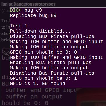
There’s currently a significant amount of confusion around the full extent of the GPIO hardware issue in the Raspberry Pi RP2350 microcontroller, with [Ian] over at [Dangerous Prototypes] of Bus Pirate fame mentioning that deliveries of the RP2350-based Bus Pirate 5XL and 6 have been put on hold while the issue is further being investigated. Recorded in the MCU’s datasheet as erratum RP2350-E9, it was originally reported as only being related to the use of internal pull-downs, but [Ian] has since demonstrated in the primary issue ticket on GitHub that the same soft latching behavior on GPIO pins occurs also without pull-downs enabled.
When we first reported on this hardware bug in the RP2350’s A2 (and likely preceding) stepping there was still a lot of confusion about what this issue meant, but so far we have seen the Bus Pirate delay and projects like [Agustín Gimenez Bernad]’s LogicAnalyzer have opted for taking the RP2350 port out back. There are also indications that the ADC and PIO peripherals are affected by this issue, with workarounds only partially able to circumvent the hardware issue.
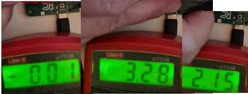
In the case of the Bus Pirate a potential workaround is the addition of 4.7 kOhm external pull-downs, but at the cost of 0.7 mA continuous load on the GPIO when pulled high and part of that when pulled low. It’s an ugly hack, but at the very least it might save existing boards. It also shows how serious a bug this is.
Meanwhile there are lively discussions about the issue on the Raspberry Pi forums, both on the E9 erratum as well as the question of when there will be a new stepping. The official statement by Raspberry Pi is still that ‘they are investigating’. Presumably there will be a Bx stepping at some point, but for now it is clear that the RP2350’s A2 stepping is probably best avoided.


Was Crowdstrike involved with the 2350s release?
B^)
If they were, all functionality would be affected only afterwards. They’d probably literally burn some fuses from the chip.
Don’t worry, hardware stuff need to have thorough simulation and testing routine in order to get even a somewhat functional prototype. Which means it is hard to skip testing when it is thoroughly baked in the process already in prototype phase.
Glad you included GuzmanBs logic analyzer.
Check out this discussion on element 14 with some really wild scope traces:
https://community.element14.com/products/raspberry-pi/f/forum/55046/rp2350-gpio-pull-down-latching-bug/223658
I hope to get to that tomorrow, but still working through PIO issues.
Ian, is there a reason the 5 XL and 6 prices are so high compared to the 5, when the BOM cost difference is so minimal (with a few buffers off the board with the 6)?
Sure: greed.
Because replacing buggy preview release hardware is baked into the plan.
“They announced that they won’t fix silicon or adapt the API, but will use documentation to deal with it.”
is this confirmed?
It would be disappointing in the extreme if this were the case. I’ve read through the primary issue which I find disturbing. Raspberry Pi Foundation should be focused on fixing the bug, not coding up word salads in an attempt to minimize it. I’ve worked with two of the reporters on other issues and neither one is prone to exaggeration.
Spoken like people who have absolutely no idea what the logistics and economics of such a thing is. It’s not software. They’ve got multiple hundreds of thousands of dollars invested in a production run and a year of lead time that they have to deal with, and undoubtedly serious negotiations and possible legal action with the IP vendor who provided the faulty silicon.
So demanding that they just snap their fingers and fix it instantaneously while simultaneously providing full details to consumers who already have demonstrated they will absolutely misunderstand anything they’re told is completely ludicrous and you should stop.
Does that mean it will take at least two years to get a fix, or is this year of lead time more like, there is a production slot assigned in a year, and it might be possible to have a revision sent it?
Depends on whether it can be fixed with an ECO or not. But it’s at least 6 months typically, and it’s VERY expensive. Even a metal (wiring only) fix needs new masks to be manufactured, which are expensive.
If they have to do a full stepping (design change, revalidate, synthesis, layout, test, full manufacturing cycle) it’s a year+ if the fab is standing around waiting to go – which of course they aren’t.
As Pelrun mentions, silicon is much harder, slower, and more expensive. It’s also much harder to valudate before production – analogue can’t really be validated by the vendor at all (without real silicon), as the tools can only simulate the digital design.
If this is an analogue issue it’s likely a bug in an external ip and nothing to do with the foundation. They then have to negotiate a fix with the ip vendor, or switch vendors (which will be a full design cycle).
By the way, no chip vendor fixes bugs if there is a way around it (e.g. dropping functionality, software/board workaround). It too expensive.
Fixing this will be quite expensive, but it’s a lesson RPi decided to learn the hard way. It was clear from the RP2040’s extensive errata list filled with clock domain crossing and quality escapes that they were in sore need for real, grown up verification in their design.
This isn’t some instant fix FPGA project, but it seems like they are more interested in blaming third party vendors than admitting that their LVS or design methodology seems quite prone to these types of amateur hour mistakes. There’s a reason we spend so much time and money on verification, because hoping for the best will cost a whole lot more down the line.
Maybe RPi learned their lesson this time.
Agreed. They should be doing better validating the digital design prior to tape out. They can also do better validating the analogue side post-silicon. They might have been able to fix this in a previous stepping if they’d found it sooner – but not if the third party vendor can’t/won’t react in time.
Having spent decades in the industry, I understand the economics all too well. I’m not demanding that they “snap their fingers and fix it instantaneously”. What I am strongly suggesting is that they do the right thing by characterizing the problem accurately and comprehensively.
It’s been shown over and over again that the loss of customer good will resulting from a botched response to an unforced error of this sort can cost much more in the long run than a single production run.
Saying that “consumers who already have demonstrated they will absolutely misunderstand anything they’re told” is both insulting and inaccurate. I sincerely hope you don’t speak for the Raspberry Pi Foundation.
There are individuals there who do indeed speak exactly like that whenever called out on things. Anyone who has encountered it will know exactly who I’m talking about.
You’re not really sounding too educated on this matter either
Raspberry Pi Ltd is for profit company making these things and the foundation is a charity.
For profit companies are going to do for profit things.
“but at the cost of 0.7 mA continuous load on the GPIO when pulled high and part of that when pulled low. “.
Those current spikes will make for a nice radio transmitter. Need more power? Just implement the workaround on more GPIO’s. It’s so easy. Congratulations RP2350 developer on your new radio project! The FCC will be contacting you with a license application shortly.
If enough of these get sold they’ll probably just include the application in the box when you buy it. Or you fill it out at checkout.
Yah right. Maybe 40 years ago. Today every light bulb is practically a radio broadcast station. Do you think we would have gotten to here if the FCC was actually enforcing things like this anymore?
Just don’t say F@#$ on the ol’ geezer’s cable TV service and you are golden.
As linked elsewhere, (https://community.element14.com/products/raspberry-pi/f/forum/55046/rp2350-gpio-pull-down-latching-bug/223658), the inputs need to be driven with a low-impedance source to overcome the 100uA peak leakage current. The leakage current is minimal outside the input voltage range of 1.3-2.4V.
So it’s totally fine for digital signals, just not for high impedance inputs.
eh…the scope traces on that forum really opened my eyes. it’s ‘good enough’ for ‘most’ digital signals but i wouldn’t say it’s totally fine for anything. it’ll at least waste a little current. i really don’t get into my workbench as much as i’d like to but even i have done some projects where i cared about this sort of thing.
like here i am with my eyes on the dallas 1-wire datasheet and i’m building an RC filter to match the curve in the datasheet — specified rise and fall times — and now they’re telling me the ‘high-impedance input’ is gonna conduct 100uA through half of my cycle? i have no doubt i could ‘work around’ it for the single bus master but if i had to deal with that on the bus clients, that 100uA would add up! i care and i don’t even use high-speed signals.
mistakes happen. and it’ll still be useful for a lot of scenarios. but this is definitely a deal breaker for a lot of digital projects. the thing that really blows my mind is that raspberry is still selling the defective chip without disclosure. they aren’t telling me. the correct process seems really obvious to me: freeze sales, freeze board production, thoroughly characterize and prominently document it, and then re-launch sales at whatever fire sale price point they think they can get away with, and negotiate with board partners whether they’ll even bother to make boards for what is presumably a sizable backstock. the most important part is that the reality shown by this oscope trace should be a canonical document from raspberry instead of a forum comment!
You’ve never had real experience with errata – there are a lot, of which many you just don’t experience.
And they will keep on selling those controllers. At a certain stage, it is like it is. Rework is seldom done, and only on selected issues.
Who did RPi foundation license the IP from? They seem to have bought a lemon GPIO block.
Who is doing the silicon fab? I heard it’s not Broadcom.
RP2040 was made by TSMC, so I’d assume the same for RP2350. I’ve not seen who the GPIO came from, only that RPi asked for a small change to be made to it and apparently got something very different back.
The Raspberry Pi folks are not pointing fingers at whoever sold them the GPIO IP, and at then end of the day, it’s their chip and their name on the line. But I bet they’re feeling pretty sore about the whole deal right now.
That said, this isn’t the first silicon bug I’ve seen in a microcontroller. I can name an erratum that I’ve personally been bitten by from every major manufacturer. Hardware is hard.
“Who is doing the silicon fab? I heard it’s not Broadcom.”
Li Wong’s Cheaper Chinese Fab House?
I thought Broadcom was fabless, at least it used to be.
Might maybe have acquired some capability when shopping around, but doubt that.
When it comes to RP’s designs, I would bet with 100% confidence they’re using the usual Foundries. Most likely TSMC simply b/c they’re the largest
Let’s not confuse GPIO and IO PAD IPs as these are quite often completely separate. Given their other peripherals like serial interfaces or USB come from Synopsys, it’s possible that GPIO and IO PAD was part of the same package deal.
In any case, issue like this are almost never caused by the IP vendor: otherwise they’d be visible in sim and on FPGA. This is most certainly an integration or manufacturing problem. Something is not given the right clock/ground or they have bunch of unexpected shorts.
What part of “got faulty silicon from an IP vendor” is bad and unethical behaviour on RPi’s part?
You’re a poor troll and you should feel bad.
The best way forward is to update the Datasheet/Errata to clearly show what’s in there and working and what not. From SW side it may also help to introduce a proper Stepping based switch which would basically remove the pull down from the API so that one doesn’t run into the problem
Latest tests show internal pull down doesnt matter, IO block is defective and latches on its own regardless. You have to use external pull downs and maybe even external buffer chips for low impedance sources. Not ideal.
Could be worse, could be an STM32. I’ve lost weeks on their undocumented SPI bugs.
I’m starting a project using SPI on a ST part? Can you possibly elaborate on the bugs?
Thank you
Robert Rother
It would be far easier if you could elaborate on which of the parts you are eyeing up.
A lot of the talk here is very much about the part errata “addendum” to the datasheet.
Most chips at the MCU level of complexity are going to have a few “quirks”.
The erratum is where the mgf will quietly tuck them away, often in a separate, obviously less promoted / showcased part of the documentation library.
For example, here is 47 pages of “quirks” for the STM32F427/437xx and STM32F429/439xx parts.
https://www.st.com/resource/en/errata_sheet/es0206-stm32f427437-and-stm32f429439-device-errata-stmicroelectronics.pdf
46 pages for the STM32F405/407xx and STM32F415/417xx device errata
https://www.st.com/resource/en/errata_sheet/es0182-stm32f405407xx-and-stm32f415417xx-device-errata-stmicroelectronics.pdf
Sixty two(!) pages for just the STM32L476xx STM32L486xx parts.
https://www.st.com/resource/en/errata_sheet/es0182-stm32f405407xx-and-stm32f415417xx-device-errata-stmicroelectronics.pdf
Welcome to the party :)
Without knowing exactly which SPI-bugs you refer to (there are plenty), I certainly know that feeling…
I’ve mostly worked with STM’s the last decade or so, and there are enough HW bugs to make grown men cry. Not to mention their HAL-FW and “Cube”-stuff; but that’s basically optional anyway.
To be fair, all MCUs, vendor-FW and tools have plenty of issues.
But accepting/doc:ing/fixing/updating HW/FW/SW-issues is, it seems, not always a very prioritized activity at some vendors…
have the DAC bug from the rp2040 been fixed?
You mean ADC right?
Yes, the spikes/noise issue was claimed to have been fixed. Haven’t seen any actual in-depth ADC performance tests yet.
And I haven’t heard if any new ADC-related issues were found
At first i groaned as the RP2350 was released just after i went and got myself a small supply of RP2040 boards for easy integrating into projects. Now i’m glad i did as the new chip is a disaster.
Like i don’t think i could trust it in any project or product for years unless they released a fixed replacement as a separate model or something.
Exaggerate, much? 🤔
Would it be an exaggeration if the OP was purchasing thousands of chips?
Well if the OP really was heavily invested, calling it a “disaster” might’ve been valid from his/her PoV at least.
Now it seems that the chip as such was unconditionally declared “a disaster” based on this errata; and that clearly seems an exaggeration to me as well.
But yeah, for the fine folks at the RP offices, it might indeed feel like a disaster. At the very least, it’s probably ruined the post-launch party mood. Probably ruined the night sleep for quite a few poor engineers too.
I would ofc agree, that if not an outright “disaster”, it’s certainly very unfortunate.
Basic I/O is so fundamental to what an MCU does, right? If, say, an integrated comparator had a HW issue – oups. Many projects perhaps won’t even need them. Or would use an external one instead. Or the ADC; bummer if there’d be an issue (like in RP2040) but for some use-cases it’d be good’nuff anyway; for others it’s OK to use an external one.
I wouldn’t call the RP2040 a ‘disaster’ even with the infamous ADC issue, would you?
(I’m in fact drafting a one-off simple design with one at this moment; ADC just for very basic supply voltage sensing, “it will be fine (probably)”… jinx, jinx)
Basic I/O is ofc much more likely to affect almost everyone. Might be good’nuff with workarounds for some, a showstopper for others.
Anyway, at least it’ll be interesting to see what, if any, details a deeper RPi analysis might reveal. If they publish anything.
I’ve got one on backorder. I just bought it because I’ve been wanting to play around with RISC-V and the other things I have are an absolute hellscape when it comes to the tool chains and documentation. I’m still really annoyed by the GPIO issues though because that really limits the usefulness to me.
Always good to wait at least six months after a new chip is released, to give time it time for the market to finding all the more obvious bugs, and get them documented, by the time you to start considering it for a product, you’re not the beta tester. All chips will have bugs… you just don’t want to have to waste a lot of development time figuring out what they are.
First off, I’ll agree that designing anything analog is hard. I work extensively with companies that design parts like this one. With proper vetting, most newer companies can get the digital logic part of their design locked down and validation on FPGAs is standard. Where things always tend to go haywire is when the digital meets the analog world. That’s where the “real-world” work begins. Leaky I/Os, oscillators that don’t oscillate, improper drive strengths, PHYs that glitch, etc.
I’m not overly familiar with the Raspberry lineup of parts. But there are some things they do well — advanced process nodes to save on die area, reduce cost, and (luckily) avoid solidly-booked process nodes supporting around 40nm supporting on-die flash which have become overbooked since the pandemic.
At a glance this issue really feels like a design/doping issue on the input buffers of the part. A standard CMOS input makes use of a pair of P & N channel FETs to invert the incoming signal as well as convert it to the correct voltage domain. Something like this (worth a quick read regardless):
https://e2e.ti.com/support/logic-group/logic/f/logic-forum/737694/faq-how-does-a-slow-or-floating-input-affect-a-cmos-device
In that picture, the leakage out of the gate of the high-side P-FET if it’s conducting can be enough to accidentally keep the N-FET partially conducting as well. Based on the symptoms reported, it seems like an input that’s high will stay there, an input that’s low will also stay there, and an input that’s in-between will sit around 50% of the supply rail. This is highly indicative of the condition described here (P&N channel doping is rarely truly symmetrical). A high input = less leakage out the gate of the FET because it’s off = less conduction by the low side FET which means the inputs will stay put. But, anything in-between will be conducting in ways that shouldn’t happen.
These inputs are supposed to have a Schmitt Trigger which means they will have hysteresis keeping them from damage when left floating partially high or low. I’m not sure how that could be working correctly in this case but a quick online search shows that it should follow a similar reasoning.
I/O can take a significant amount of die area in advanced process nodes because the transistors needed to interface to the outside world can’t shrink to the same extent that the internal digital logic can. Hopefully what happened here is that the the Pi folks didn’t test enough of the “corner lots” (process variation) and only some of their devices snuck out experiencing this issue. Hopefully they can change the doping parameters using their existing metal masks and turn out parts where the gates of their FETs leak less and therefore can actually have the inputs states defined by the built-in pull resistors.
IF that’s the case, then a full fix could be mere months away (including full validation this time). Hopefully it gets followed up with a manufacturing date code break to guarantee the ability to buy parts that behave normally.
Seems like their focus on the computing side had distracted them from proper testing of the i/o portion.
The errata has been updated per https://github.com/raspberrypi/pico-feedback/issues/401#issuecomment-2334490720
The root cause seems to be that the input pins are sourcing around 120 microamps of current when their voltage isn’t at GND or Vcc. I think this explains the symptoms people are seeing, and it’s a shame because this can lead to increased power draw. Although, the errata claims that it’s possible to stop the leakage by disabling the input pin until a read is needed. I’m… not sure how this will work with GPIO interrupts. Another option is to place a pull-up or a very strong pulldown resistor.
Re. GPIO interrupts :
I would assume, a strong buffer e.g. op-amp to make the src signal(s) low-impedance enough to not be affected by the leakage.
So while the errata doesn’t have to be a show-stopper, the workarounds might add cost (external components & area), power & complexity.
Disabling inputs except for periodic sampling might be acceptable in some cases, but I’d label that as ‘added complexity’ at least.
I’ve found two similar issues with E9:
a) It hangs also at 2.2V without (!) any pull-resistor enabled (e.g. changing the direction, from OUT to IN, e.g. for a bi-directional signal like on MDIO). But with an external driver (or “stronger” pull-down) – it solves the issue (so, E9 errata sounds correct). “Don’t let inputs be floating”.
b) More concerning for me: I have figured out today: the maximum speed for a synchronous, full-duplex interface (such as SPI) is limited to 25MHz.
Input pins seem to have a large delay (before the external signal reaches the internal logic), e.g. 30ns (I assume to see it).
Tested, verified, via a PIO SPI implementation: anything above 25MHz fails (with bit errors: MISO is sampled at a “delayed time”, internally).
My suspicion: if this is a general issue on any GPIO input, also for “native SPI peripheral” pins? – a SPI cannot be faster as 25 MHz (even technically possible up to SYSCLK/2 = 75 MHz).
Doing a simple MOSI – MISO loopback – bit errors above 25MHz (caused by a too much delayed input MISO signal). This GPIO input delay concerns me more.