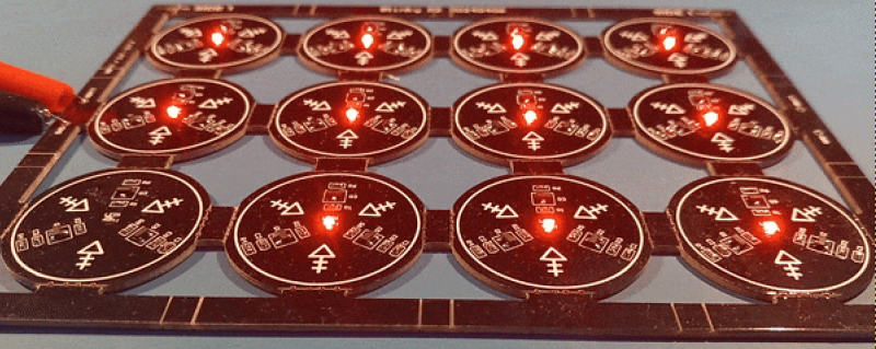
We might consider PCB panels as simply an intermediate step towards getting your PCBs manufactured on the scale of hundreds. This is due to, typically, an inability to run traces beyond your board – and most panel generators don’t give you the option, either. However, if you go for hand-crafted panels or modify a KiKit-created panel, you can easily add extra elements – for instance, why not add vias in the V-Cut path to preserve electrical connectivity between your boards?
[Adam Gulyas] went out and tried just that, and it’s a wonderfully viable method. He shows us how to calculate the via size to be just right given V-Cut and drilling tolerances, and then demonstrates design of an example board with discrete component LED blinkers you can power off a coin cell. The panel gets sent off to be manufactured and assembled, but don’t break the boards apart just yet — connect power to the two through-hole testpoints on the frame, and watch your panel light up all at once.
It’s a flashy demonstration – even more so once you put light-diffusing spheres on top of the domes. You could always do such a trick with mousebites, but you risk having the tracks tear off the board, and, V-Cuts are no doubt the cleanest way to panelize – no edge cleaning is required after breaking the boards apart. Want to learn about panel design? We’ve written and featured multiple guides for you over the years.


I often do something similar at work. But not with V-cuts, as this is too fragile in my opinion.
I use mousebites and route power, GND and SWD through small traces on the inner layers between the mousebite holes. I then use a WE WR-WST REDFIT connector that I plug into the frame to connect the whole panel to my programming adapter and flash and test all boards at once.
This is what I am used to as well. First time I saw it used was in 1999 at the contract manufacturer I was working at. A video company was making small handheld devices that utilized this method for programming, self test, and the first round of burn-in. It allowed us to have confidence to test as a panelized board, complete the entire assembly process, and then only do a quick final test before shipment.
No edge cleaning for V-cuts? Pfft, hardly! Fiberglass strands stick out aplenty, so a bit of sanding is in order.
In automotive we would be crucified to have exposed coper on the de-paneled pcb. There’s even a inspection point on the end of each line just for that
Indeed, exposed copper is an oxydation risk.
By the way I would love an article about conformal coating best practices.
don’t, its a nightmare with stinky chemicals that always dries out right before you try to run
Well I ment industrial application and DFM.
I’ve got multiple design, mass produced, with either manual and automated application, but it’s always a compromise of cost, clearance, connector choice, switch, manual labor, repairability, etc.
I can give a shot at it if the editorial team is interested.
If you write up your stories/guidance/tips, please do send them in! ^~^ publish them somewhere online, even a .txt (or better, a .md) in a github repo will do, and send it as a tip, I’ll be on the lookout for it!
Mousebites and V-cuts are new terms for me, although I had an idea what they mean. This link clarified them for me.
https://www.nextpcb.com/blog/complete-guide-to-pcb-stamp-holes