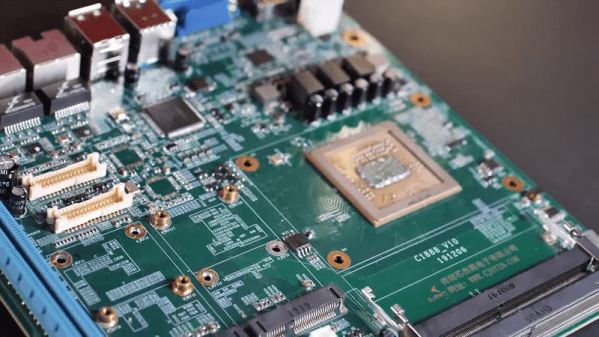
PCB internal bodge

PCB Microsurgery Puts The Bodges Inside The Board

We all make mistakes, and there’s no shame in having to bodge a printed circuit board to fix a mistake. Most of us are content with cutting a trace or two with an Xacto or adding a bit of jumper wire to make the circuit work. Very few of us, however, will decide to literally do our bodges inside the PCB itself.

The story is that [Andrew Zonenberg] was asked to pitch in debugging some incredibly small PCBs for a prototype dev board that plugs directly into a USB jack. The six-layer boards are very dense, with a forest of blind vias. The Twitter thread details the debugging process, which ended up finding a blind via on layer two shorted to a power rail, and another via shorted to ground. It also has some beautiful shots of [Andrew]’s “mechanical tomography” method of visualizing layers by slowly grinding down the surface of the board.

[Andrew] has only tackled one of the bodges at the time of writing, but it has to be seen to be believed. It started with milling away the PCB to get access to the blind via using a ridiculously small end mill. The cavity [Andrew] milled ended up being only about 480 μm by 600 μm and only went partially through a 0.8-mm thick board, but it was enough to resolve the internal short and add an internal bodge to fix a trace that was damaged during milling. The cavity was then filled up with epoxy resin to stabilize the repair.

This kind of debugging and repair skill just boggles the mind. It reminds us a bit of these internal chip-soldering repairs, but taken to another level entirely. We can’t wait to see what the second repair looks like, and whether the prototype for this dev board can be salvaged.

Thanks to [esclear] for the heads up on this one.

DIY castellated PCB connectors

Snip Your Way To DIY PCB Castellations

Castellated PCB edges are kind of magical. The plated semicircular features are a way to make a solid, low-profile connection from one board to another, and the way solder flows into them is deeply satisfying. But adding them to a PCB design isn’t always cheap. No worries there — you can make your own castellations with this quick and easy hack.

Scissors cutting a PCB through vias to make castellations[@CoilProtogen] doesn’t include much information in the Twitter thread about design details, but the pictures make it clear what the idea is here. OEM castellations are really just plated areas at the edge of a board that can be used to tack the board down to another one without any added hardware. The hack here is realizing that lining up a bunch of large-diameter vias and cleaving them in half with a sharp pair of scissors will result in the same profile without the added cost. The comments on the thread range from extolling the brilliance of this idea to cringing over the potential damage to the board, but [@CoilProtogen] insists that the 0.6-mm substrate cuts like butter. We’d worry that the plating on the vias would perhaps tear, but that seems not to be the case here.

The benefits of a zero-profile connection are pretty clear in this case, where castellated PCBs were used to replace bulky header-pin connectors on a larger PCB. We can see this technique being generally useful; we’ve seen them used to good effect before, and this is a technique we’ll keep in mind for later.

Open-Source Method Makes Possible Two-Layer PCBs With Through-Plating At Home

If the last year and its supply chain problems have taught us anything, it’s the value of having a Plan B, even for something as commoditized as PCB manufacturing has become. If you’re not able to get a PCB made commercially, you might have to make one yourself, and being able to DIY a dual-layer board with plated-through vias might just be a survival skill worth learning.

Granted, [Hydrogen Time]’s open-source method, which he calls “Process 01”, is something that he has been working on for years now. And it’s quite the feat of chemistry, which may require you to climb a steep learning curve, depending on how neglected the skills from high school or college chemistry are. But for as complex as Process 01 is, it’s actually pretty straightforward, and the first video below covers it in extreme detail. It starts with a drilled double-sided copper-clad board, which after cleaning is given a bath in palladium chloride. A follow-up dunk in stannous chloride leaves a thin film of palladium metal over all surfaces, even the via walls. This then acts as a catalyst for electroless copper plating in a solution of copper sulfate, followed by an actual electroplating step to thicken the copper plating.

After more washing, photoresist is applied to define the traces as well as to protect the now-plated vias, the board is etched, and a solder mask layer is applied. The boards might not be mistaken for commercial PCBs, but they’re pretty darn good, and as [Hydrogen Time] states, Process 01 is only a beginning. We expect this will be improved and streamlined as time goes by.

Fair warning, though — some steps require a fume hood to be performed safely. Luckily, we’ve got that covered. Sort of.

Continue reading “Open-Source Method Makes Possible Two-Layer PCBs With Through-Plating At Home”

China X86 Chips Hitting The Market

Last year, fabless chip maker Zhaoxin announced they were readying a multicore x86-compatible CPU. According to media reports, the chips are showing up on Chinese marketplaces like Taobao shipping around March.

The company is a joint venture between the Shanghai Municipal Government and VIA Technologies, a familiar name in the PC business. It makes even more sense if you remember that VIA bought Centaur who had built simple x86 chips and used the simplicity to add more cache that more complex Intel and AMD chips. These fell out of the hobby market, but they’ve still been pushing forward providing simple designs that are inexpensive and consume low power.

Continue reading “China X86 Chips Hitting The Market”

Nixie Clock Failure Analysis, [Dalibor Farný] Style

We’ve become sadly accustomed to consumer devices that seem to give up the ghost right after the warranty period expires. And even when we get “lucky” and the device fails while it’s still covered, chances are that there will be no attempt to repair it; the unit will be replaced with a new one, and the failed one will get pitched in the e-waste bin.

Not every manufacturer takes this approach, however. When premium quality is the keystone of your brand, you need to take field failures seriously. [Dalibor Farný], maker of high-end Nixie tubes and the sleek, sophisticated clocks they plug into, realizes this, and a new video goes into depth about the process he uses to diagnose issues and prevent them in the future.

One clock with a digit stuck off was traced to via failure by barrel fatigue, or the board material cracking inside the via hole and breaking the plated-through copper. This prompted a board redesign to increase the diameter of all the vias, eliminating that failure mode. Another clock had a digit stuck on, which ended up being a short to ground caused by pin misalignment; when the tube was plugged in, the pins slipped and scraped some solder off the socket and onto the ground plane of the board. That resulted in another redesign that not only fixed the problem by eliminating the ground plane on the upper side of the board, but also improved the aesthetics of the board dramatically.

As with all things [Dalibor], the video is a feast for the eyes with the warm orange glow in the polished glass and chrome tubes contrasting with the bead-blasted aluminum chassis. If you haven’t watched the “making of” video yet, you’ve got to check that out too.

Continue reading “Nixie Clock Failure Analysis, [Dalibor Farný] Style”

Fail Of The Week: How Not To Light Pipe

You’d think that something made out of glass and epoxy would transmit a decent amount of light. Unfortunately for [Jeremy Ruhland], it turns out that FR4 is not great light pipe material, at least in one dimension.

The backstory on this has to do with #badgelife, where it has become popular to reverse mount SMD LEDs on areas of PCBs that are devoid of masking, allowing the light to shine through with a warm, diffuse glow – we’ve even featured a through-PCB word clock that uses a similar technique to wonderful effect. [Jeremy]’s idea was to use 0603 SMD LEDs mounted inside non-plated through-holes to illuminate the interior of the board edgewise. It seems like a great idea, almost like the diffusers used to illuminate flat displays from the edge.

Sadly, the light from [Jeremy]’s LEDs just didn’t make it very far into the FR4 before being absorbed – about 15 mm max. That makes for an underwhelming appearance, but all is certainly not lost. Valuable lessons about PCB design were had, like exactly how to get a fab to understand what you’re trying to do with non-plated holes and why you want to fence the entire edge of the board in vias. But best of all, [Jeremy] explored what’s possible with Oreo construction, and came away with ideas for other uses of the method. That counts as a win in our book.

CNC Machine Most Satisfyingly Mills Double-Sided PCBs

We know that by this point in the development of CNC technology, nothing should amaze us. We’ve seen CNC machines perform feats of precision that shouldn’t be possible, whether it be milling a complex jet engine turbine blade or just squirting out hot plastic. But you’ve just got to watch this PCB milling CNC machine go through its paces!

The machine is from an outfit called WEGSTR, based in the Czech Republic. While it appears to be optimized for PCB milling and drilling, the company also shows it milling metals, wood, plastic, and even glass. The first video below shows the machine milling 0.1 mm traces in FR4; the scale of the operation only becomes apparent when a gigantic toothbrush enters the frame to clear away a little swarf. As if that weren’t enough, the machine then cuts traces on the other side of the board; vias created by filling drilled holes with copper rivets and peening them over with a mandrel and a few light hammer taps connect the two sides.

Prefer your boards with solder resist and silkscreening? Not a problem, at least judging by the second video, which shows a finished board getting coated with UV-cure resist and then having the machine mill away just the resist on the solder pads. We’re not sure how they deal with variations in board thickness or warping, but they sure have it dialed in. Regardless of how they optimized the process, it’s a pleasure to watch.

At about $2,600, these are not cheap machines, but they may make sense for someone needing high-quality boards with rapid turnaround. And who’s to say a DIY machine couldn’t do as good a job? We’ve seen plenty of them before, and covered the pros and cons of etching versus milling too.

Continue reading “CNC Machine Most Satisfyingly Mills Double-Sided PCBs”