There’s a new Python-based script that will panelize your KiCad circuit boards from the command line. The project by [Jan Mrázek] is called KiKit and works on .kicad_pcb files to arrange them in a grid with your choice of mousebites or v-cuts for separating the boards after production.
When working with smaller boards it’s common practice to group them together into panels. This is done to speed up PCB assembly as multiple boards can have solder paste applied, go through a pick and place machine, and be sent into the reflow oven as a single unit. Often this is done manually, but in many cases this script will save you the time while delivering the results you need.
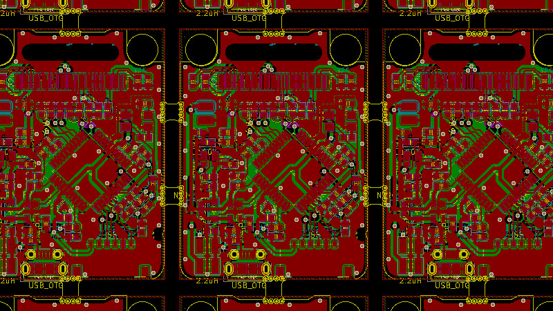
Let’s say you really wanted to make a whole bunch of those Xling open source Tamagotchi-like key fobs we saw a couple of weeks back. Using KiKit you can gang up six of the boards at a time, using “mousebites” to keep them together during production but make it easy to separate them after all the components are soldered:
/usr/local/bin/kikit panelize grid --space 3 --gridsize 2 3 --tabwidth 3 --tabheight 3 --htabs 2 --vtabs 1 --mousebites 0.5 1 0.25 --radius 1 Xling/hardware/xling.kicad_pcb xling_panel.kicad_pcb
You can see that the parameters let you set space between the boards, number of boards in the grid, width of the tabs, tab dimensions, number of tabs between boards, and even the radius of the curve where the tabs meet the board. These settings were pulled from the examples page, which demonstrates outcomes for many different settings options.
 If you want to give this a try, we suggest installing directly from the repository, as improvements are ongoing and the pip3 version didn’t have all of the options shown in the examples. For us this was as easy as
 sudo python3 setup.py install and then calling the script with the full path /usr/local/bin/kikit.
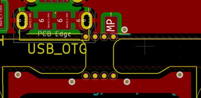
Results from this board are both impressive and cautionary. You can see the top edge of the design is recessed yet the most up-to-date version of KiKit was still able to make the connection. However, how this affects the USB connector on the bottom of the board design may be something to consider before pulling the trigger on your panel order.


If only KiCAD had panalization in it already…
Though, running a script like this at least bridges that gap in functionality in the mean time.
Sure is a lot better then how I currently do panelization.
I currently copy the whole project, add “panel” to the end of the project name.
Then I go into PCBnew and use the array tool to create the desired panel. Of course this means I need to do all V groving and mouse bits manually….
I also keep the two projects in a directory for that project/revision. A fair bit of manual work, but currently not all to much hassle, and gives decent results, not to mention that I can be very picky about where exactly I put the mouse bits.
You can also be picky about tab placement with KiKit. Just write few lines of Python code to describe your panel and your ready to go. KiKit is designed mainly as a library for easy panelization – it does all the heavy lifting of board substrate merging, KiCAD confusing API handling and abstraction about cuts for you. The CLI only covers the basic and the most common use cases – if the CLI should cover it all, you would basically came up witch custom language and.. why not use an existing one – Python?
Also, KiKit makes the work repeatable – once you change your board, you just call make and with no effort you get your panels. No change for making a silly mistake in you panel…
I’ll take it. Better than nothing. I’ve been using the free Gerber panelizer from http://blog.thisisnotrocketscience.nl/projects/pcb-panelizer/ but that is Windows only and major PITA to get it to work. Also you can’t edit the PCB afterwards.
For large (huge) software like Kicad I prefer a less monolithic approach. Plug ins are fine.
Same with gimp
The decision between a plug in heavy or monolithic program design is a debatable topic.
Though, both design approaches could be abhorrent if poorly implemented….
A poorly implemented monolithic one will just be crude to use, while a wild western free for all plugin based program would be an error ridden trail to hike, due to plugins conflicting with each other…
If properly implemented, they can both be wonderful to worth with.
Though, panelization is such a standard procedure in PCB manufacturing that it should probably be part of KiCAD.
For all the more niche things, plugins makes a lot of sense.
Nope. There is an interface to a standalone package FreeRrouting – I’ve had some success with it in the past, but sometimes it gets stuck and you have to move things around to help it.
I believe that most of the designers want to route boards themselves only novice wants to use autoroute.
You can always route critical stuff by hand and leave the rest to autorouter… Still very usefull.
Not going to lie, I haven’t seen anyone using autorouters professionally
Would like to see some video tutorials on such a work flow.
Wow, great job! It exceeded my expectations. It can even make tabs with mousebites on rounded edges/corners.
I have found only one issue: because all arcs are transformed into polylines, some holes are sometimes missing due to asymmetry. Is there any parameter to change the number of segments to which arcs are transformed?
After consultation with Honza, this issue with missing holes is already fixed in current master build. And there will be new stable release in a few days.
Due to licensing issues the autorouter is not distributed with kicad, but it is easy enough to download separately and then it integrates itself into the board layout tool.
https://freerouting.org/freerouting/using-with-kicad
With a board panelized using KiKit is a POS/CPL file produced? If not is there another tool to create a POS file for the panel?