
The software and hardware worlds have overlaps, and it’s worth looking over the fence to see if there’s anything you missed. You might’ve already noticed that we hackers use PCB modules and devboards in the same way that programmers might use libraries and frameworks. You’ll find way more parallels if you think about it.
Building blocks are about belonging to a community, being able to draw from it. Sometimes it’s a community of one, but you might just find that building blocks help you reach other people easily, touching upon common elements between projects that both you and some other hacker might be planning out. With every building block, you make your or someone else’s next project quicker, and maybe you make it possible.
Sometimes, however, building blocks are about being lazy.
Just Throw Pin Headers
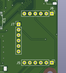
Back when I was giving design review on a LVDS driver board for a Sony Vaio display, there was a snag – the display used, doesn’t generate its own backlight voltage, so you have to bring your own backlight driver. Well, I didn’t want to bother designing the backlight driver portion of the circuit.
 The way I justified it, adding that circuit to the board didn’t make much sense – the entire board was an experimental circuit, and adding one more experiment onto it would result in extra board revisions and reassemblies. Honestly, though, I just really didn’t want to design the LED driver circuit at the time – it didn’t feel as interesting.
So, I had an easy-to-follow proposal – let’s put all backlight-driver-related signals onto three pin headers, forming a “module” footprint of sorts, and then develop the module separately! The hacker agreed, and in the meantime, used a spare panel’s LED backlight to test the display in the meantime – way more accessible of a solution. The pin headers remained, at the time, bound to be unpopulated for, at least, until the next PCB order.
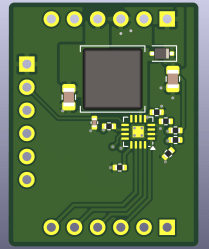
New revisions of the module came and went, now bearing a HDMI port and a whole new ASIC – easy to design, because, again, the hacker didn’t have to worry about the backlight circuit, and just kept the module footprint from the previous design. Was the backlight driver module PCB designed yet? Well, simply put, no.
 A friend of mine, just a month later, was designing a motherboard replacement for a tablet computer, and she asked me for advice on how to power the backlight. I thought for a second, and, I had an easy answer for her – use the module footprint. At that point, I still haven’t designed the module, but I didn’t have to mention that. She rejoiced, put the module footprint onto the board, even designed her own neat symbol for it, and then promptly went on to lay out diffpairs and reverse-engineer pinouts, both significantly more fun activities than designing a backlight driver with zero experience in design of backlight drivers.
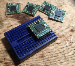
Some time later, I started getting insistent messages from the original hacker, about needing a backlight driver. The funny part is that by that point, I have already had designed a backlight driver circuit for my own Vaio motherboard, but I never felt engaged enough to turn it into a module. A different friend of mine was looking for small projects, however. I gave her the task: here’s a footprint for a module, here’s a circuit that goes onto the module, and we need a module. Indeed, she has delivered a module – by that point, a module we could put onto three different PCBs.
Building Blocks
The entire occasion definitely helped cement my reputation as someone who delivers, eventually – with big emphasis on eventually. It also brought four people and three projects together, and it let us order the first revision PCB way sooner than otherwise, all because we set out to eventually add the backlight circuit as a module. Now, this module is a building block in our projects – whenever one of us, or maybe one of you, needs a backlight driver, we know that we have an option handy.
I have some unique experiences with PCB modules as building blocks – at one point, I’ve built an entire phone out of them, and I still build devices heavily based on modules. Whenever I’d have the occasion, I’d throw a TP4056 module footprint onto a board instead of reimplementing the whole circuit from scratch. In 2022, I designed a module with a RP2040 and the FUSB302 USB-PD PHY – it was the building block that led to my USB-C series on Hackaday, and eventually helped me, my friends, and other hackers develop a whole lineup of unique USB-C devices.


Building block use and design is the fun way, and it’s the lazy way, and it’s the friendly way – would you believe me if I told you it’s also the safe way? Say, does your circuit need a custom DC-DC, or can you slap a few pads onto the board to connect a commonplace generic module? If you can afford the increased space, might as well make your board as simple as it goes – if there’s less to test and bringup, you’ll get to your project’s finish line earlier, and have less hurdles to jump over.
The Practical Aspects
There are a few techniques you can use if you want to make a building block – pin headers are the simple obvious one. Castellations is a fun one, and here’s a trick – you don’t have to pay JLCPCB for castellated holes, as long as you are fine getting dirty ones, which are still wonderful for prototyping. If you’re using Aisler, you can get perfect castellated holes, though – good for scaling up a module of yours after you’ve verified the design. Don’t be scared of turning through-holes into castellations – it works, and it’s super easy if your board is thin enough. Oh, and you might just be able to get castellations through V-Cuts!
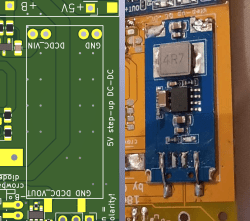
Got an Eastern or Western module, and it doesn’t quite use pin headers? Get out the calipers, measure its pads, and create a footprint for it – you will thank yourself later. I’ve done just once for a 5 V boost module, stocking up on them and putting them onto a bunch of boards. It’s not like I’d feel comfortable designing 5 V boost regulators at the time, so the module has bought me a couple years of worrying about something else instead. The modules have since vanished from the market, but, today I’ve got a few 5 V boost designs I can easily make modules out of. Now, it looks like I can even upgrade my own old boards that are still in use!
When designing your own boards, try to put all pin headers on a grid, 2.54 mm (0.1in) is a must – only use an integer millimeter grid or pin headers if you have no other options. Such a module isn’t just solderable – it’s breadboardable, which helps a ton when you’re trying to figure out an especially daring circuit technique. Castellated modules can be breadboardable, too, if you make sure to concentrate the core necessary signals on two opposite sides!


Are you designing a new module for your own use? See if there’s a footprint you can copy, or an unspoken standard you can follow. Boards speak about themselves through their looks, and footprints convey a purpose through their layout. Look at the boards above- it’s pretty easy to notice that they are TP4056 style battery chargers, but all of them upgraded in their own way. If you follow an existing footprint when designing your own board, it’s going to look more familiar for a newcomer hacker, channeling the power of skeuomorphism where you might not have expected to find it.
The Looks Make The Module
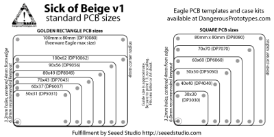
Board formats are underrated when it comes to accidentally creating building blocks. Sparkfun has example layouts for QWIIC devices – follow it, plop a JST-SH connector on, maybe order your PCB in red for a change, and your sensor PCB will shine in a whole new way in your eyes. Dangerous Prototypes, on the other hand, suggests a set of PCB formats known as Sick of Beige that work with existing enclosures and lasercut templates – that’s the surface-level benefit, the real deal is that these footprints also talk the Dangerous Prototypes language. If your programmer board feels like a generic rectangle, putting it into the frame of BusPirate fame will give it the air of hacker-oriented tooling. With both of these formats, you get mounting holes – mark of a hacker who knows what’s good.
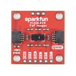
Interconnect standards go hand in hand with making your building blocks’ features recognizable without reading the silkscreen – it’s why I talk so much about QWIIC, and a JST-SH connector is always a welcome addition on my boards. Adding a well-recognized standard connector makes your board recognizable as a potential building block. Now, the board looks interoperable if you just give it a chance, equipped with a familiar socket, and perhaps, you won’t feel as much need for designing a new one – quite likely, building a new device in a single day instead of two weeks’ time.
Sometimes, your board will be split apart into building blocks without your involvement whatsoever. Publishing a design that goes beyond connecting a button to an LED? Try to fill in the blanks – it’s about helping the hacker that follows in your footsteps. Sometimes it’s a highschool kid trying to put together a design, and sometimes it’ll be you again, just a couple years later. So, note down the part number of that switcher inductor in the schematic, and fill in the values of the resistor divider while you’re at it – and if you’re revisiting a board of yours where you haven’t done that, do it, then git commit and git push.
Beyond The Ordinary
There’s building blocks everywhere for those with the eyes to see. A single-board computer is one, I’d argue – a SoM in a DDR footprint is one without a doubt. An engineer once showed me a technique for creating building blocks out of thin air – taking unpopulated leftover large project PCBs, then sawing out the section with the circuit you need. Sometimes, you really only need a single piece of that one Ethernet transceiver circuit, and you need it now – you might have not planned for it, but the Dremel tool forgives all.
Circuit blocks are an often requested feature in KiCad. At the moment, you can copy-paste portions of a schematic between projects – which is more than good enough for many circuits. It’s not as great for switching regulators or MCUs, however, and we can’t help but hope to see new advancements in the field soon. Perhaps, one day, you’ll be able to click a few buttons and turn your favourite USB hub into a circuit block – and from there, who knows, maybe you can fill the void that the NanoHub’s eternal out-of-stock state has left in our hearts!


I use the pin header method with a lot of small boards. The small boards get combined into larger projects with wiring harnesses. The biggest drawback is that wiring harnesses get large and complex. It’s still a great way to prototype or make proof of concept type projects.
Have done a few projects where a small module gets plugged into a larger board, but that method means that you are paying twice for the same PCB real estate.
How hard would it be to come up with a hobby standard of module pinouts..
like small/medium/big
e.g. ?/mikroBUS/arduino pinout
Good question! Quite a bit would depend on the scope, it feels like. Quite a few ad-hoc standards are unintentionally developed by Adafruit/Sparkfun/Seeedstudio and co, I think – they have the QWIIC/Stemma, the Lilypad wearable sensor lineup, it’s all quite endearing. Now that you bring it up, I wish I touched upon standards like mikroBUS in this article – sadly, I might not have the structure to hang these onto!
There’s an XKCD for this.
On my desk right now, I have I2C sensors that are pinned out VCC GND SCL SDA, VCC SCL SDA GND, … etc. Two of them (accidentally?) match.
https://hackaday.com/2022/05/04/the-connector-zoo-i2c-ecosystems/
https://hackaday.com/2016/11/09/my-life-in-the-connector-zoo/
I still like PMOD, but it’s soo big.
Or olimex’s UEXT!
You remind me of the Arduino connector standard, that includes a +5V power line and (traditionally) 5V logic levels. Often seen on FPGA based dev boards, where the main chip is NOT 5V tolerant.
0.1 inch style header connectors also tend to have clock speed limits.
So your “standard” needs to start by specifying a voltage level, and a maximum clock speed.
3.3-150 is 3.3V @ 150MHz, for example. You probably need an impedance spec as well, to avoid reflected signals on PCB traces.
some how ive gone from custom home-etched boards to masses of dev boards attached to a 3d printed frame with jumper wires connecting everything. one would think i would progress the other way, or used a pcb service.
ultimately its a logistics problem. living in a small town in alaska i just cant get parts locally, and i am spending most of my hack money on shipping. so when it comes to buying a hundred different parts from 10 different stores, or buying a few knockoff dev boards from china (sometimes sparkfun or adafruit but they are overpriced, and the latter has horrible shipping terms to ak), gluing dev boards together wins out.
Mounting holes FTW!
Also, put 0.1″ header holes over solderable jumper pads, enabling permanent or changable settings of the jumper.
Likewise, 0.1″ header pattern over USB connector pads; flexibility whether to use the connector.
Imagine the ways a module might be hacked, then overlay header holes there.
I would even argue breakouts/modules/blocks became pretty much the go to method for any hobbyist. Especially with the rise of the Arduino and the easy use of its libraries.
Just yesterday i opened up a project a few interns here did. Some servos, sensors, displays, etc…. all modules from adafruit and co. connected to an Arduino.
Where back in the day we would have made a custom pcb and get headaces when one part wont work or breaks.
I know they did for me. Unless I have sensible contraints (space, etc) I will chain together modules wherever possible.
I don’t need to reinvent the wheel for clout, I need something suitable for the task. Sure I could design something cheaper, but my time also has value.
I think these last couple of decades of making little modules for everything has been excellent.
Yea, developing a commonly used sub-circuit as a module speeds up prototyping. I can order a pile of PCBs for a small PSU, fab several of them excepting the parts that define the output voltage (put these somewhere they’re easy to add last). I have a small switcher module that is pinned the same as common TO220 linear regulators: IN-GND-OUT, and have several of them pre-assembled for 5V and 3V3 to use for prototyping
When laying out something for generic use, consider the possibility of signals which could be useful but might not be used in every situation. What you’re making today might not provide an EN signal for the module, but if you provide an optional pin for it, and on the module can short Vin (or whatever) to that signal with a 0R (or the host project can have a trace doing the same) so that if it’s powered, it’s just enabled, but if you have a project where there’s a benefit to be had by controlling an EN pin, that can be facilitated.
Setting up breadboard friendly pin spacing and alignment certainly makes them friendlier to use by your friends who use breadboards (I largely avoid them due to capacitance and iffy connection reliability when using different gauge components). Obviously, if you have some pin headers coming out the top or side of a PCB, for connecting to through a header, those might not need to be aligned.
In a similar vein relative to module use for various projects, I have boards which sport multiple configuration options – two or three different regulation paths (Zener did you say? linear reg? switcher? bypass, expecting offboard regulation?), a couple of power inputs (barrel, pin header), etc. onboard PWM generation, or mcu provided PWM, or no PWM at all? This gives me options when I go to use the board. Of course, not all of the parts need to be populated. Creative tapered footprints allow for some parts to be different package sizes depending on what you have on hand. Parallel resistor pads allow for tuning a design (handy for current sense).
I have a mains switching board, originally designed with a MCU onboard when I made the home etch prototype (which itself is still in service). When I laid out the one for the PCB order, I routed all the MCU pins out to a no-populate row of TH for a pin header. Subsequently, I used a PCB without an MCU, instead connecting a small home-etch PCB with a comparator and external thermistor to control a fan in a decidedly more analog fashion (though I could have used an MCU and connected a thermistor to a power pin and an unused ADC pin). Designing some projects with an eye for using them for projects you didn’t have in mind when you did the initial design can be just as useful as them being a generic supply or driver. A little brainstorming up front can make the extra boards you get from some small PCB order serve other potential functions, or provide justification to order a lot more of some design.
It sure seems Sick of Beige case components have turned into vapor ware. I’ll stick with Eurocard 100x80mm where appropriate I guess.