Ordering a PCB with mistakes sucks. We should help each other avoid such mistakes – especially newcomers. One of the best ways to avoid these mistakes, especially if it’s your first one, is to get a few other people to look at it. You deserve to get a PCB that is as functional and as helpful as humanly possible, so that you can be happy with your project, and feel ever so slightly more confident in yourself in whatever you shall set out to do next.
At the end of last year, I put out a call for design review submissions, and we’ve received enough projects to make me feel overwhelmed for a bit. A design review has always felt like a personal thing, and here we are doing them in public. But in that sense, we hope that everyone can learn from them, and we hope to push forward a healthy review culture.
What’s more, these articles won’t just be design review. Every project I’m highlighting is worthy of a Hackaday feature just on its own, so tune in and learn more about them!
Today’s Contestant
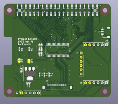
For this example, I will be walking through a review I’ve already given someone with a pretty cool board, for a pretty cool project I’ve already shown you. Remember the Sony Vaio remake project? A fair bit of people have reached out to me afterwards, and one of them, [Exentio] also had the same Sony Vaio rebuild idea in mind. We started chatting, and he decided to tackle one of the project’s milestones, and perhaps the most crucial one – adapting the LCD.
The stock LCD in the Vaio is LVDS, and the Raspberry Pi boards we’ve agreed on using don’t have that – they have parallel RGB, HDMI and DSI display interfaces available. Plus, it has non-standard display backlight arrangement, as the backlight driver is expected to be on the mainboard. This complicates things compared to most displays on the market, where you just provide a hefty voltage rail and a few board signals.
Our hacker has done wonderfully with the first revision, and there’s visibly a lot of care put into routing, even length matching the parallel RGB interface, which isn’t required but is definitely a nice thing to do. The star of the show, a parallel RGB chip from TI, is correctly wired up – I’ve checked both the datasheet and the Raspberry Pi parallel RGB (DPI) mappings! It’s a great example of a board that’s going to work for its purpose.
It’s also a great example of a board you could make even more helpful than it already is! [Exentio] sent me a .zip file with the board as it was initially, we hopped on a Discord screenshare call, I would speak in voice chat, [Exentio] would type in text chat, and I’ll walk you through what we talked about. For a start, let’s talk about component choices.
More Friendly Components
The board has a lot of different components, and I’m not convinced that all of them are optimal. This board uses comparably large tantalum caps at the regulator, but then has 0201 resistors and 100 nF capacitors for the chip. We talked about it, and it turned out they made a KiCad-aided mistake of picking the “R/C_0201_0603Metric” footprints, thinking they’d be what we actually mean when we recommend 0603. But 0603 in imperial units is a lot bigger than 0603 metric! Eventually, you learn to notice such mistakes early – otherwise, that’s what a review is for!
The tantalum capacitors at the 1117 are also not as friendly. For a start, the 1117 is an outdated regulator design, which requires you to use high-ESR capacitors, and usually, electrolytic caps. Tantalum caps tend to be the opposite of high-ESR, so the regulator will struggle. Of course, this is just a footprint, and you could also solder ceramic capacitors onto it – except they’re also not going to work. Switching to a more modern regulator will fix it, and the best part is we will barely even have to change the circuit!
 For context, this linear regulator generates a 2.5 V rail for the display’s logic power rail. A linear regulator is a great choice for this task, since the current will be less than 1 A, which is about where such linear regulators start to underperform. There are many linear regulators that can handle such work, and what’s best, they are package- and pinout-compatible with the old 1117 regulators! I recommended the AP2111 or AP2114 in particular – easy to find on both Mouser and LCSC, and both have 2.5 V versions.
Finally, powering this regulator from the Pi’s 3.3 V rail is a better bet, because you can then reduce the amount of voltage dropped by the regulator. A 3.3 V to 2.5 V drop wouldn’t work with 1117, but our new regulator can do that without a worry! A possible issue with this is that different Pi boards have different current capacities on the 3.3 V rail, so a display like this could perhaps overcurrent the rail. If that fails us, however, we could also rewire the regulator back to 5 V without a worry.
As for the RGBTTL-LVDS chip, it’s a great pick – there are some slightly cheaper ones, but honestly, the savings are not worth the reroute. Also, it makes sense to build this board around a known-working high-quality chip from TI. The fewer assumptions your board design relies on, the better, and adding a less tested chip is a gamble we don’t have to pull today. Instead, let’s make sure this board does as much for us as it can!
Sanity Checks
Any time chips can interface with each other in multiple modes, there is an opportunity for mistakes. Here, that’s wiring between the DPI interface GPIO mappings and the few different ways you can wire up. I sat down, checked this particular schematic, and it was perfect! When you’re doing such a check, I recommend making a table you can cross-compare, maybe in the schematic editor using text labels, or in Excel – wherever is more comfortable for you, the most important thing is that you don’t need to rewire the tiny pins of the parallel RGB interface IC.
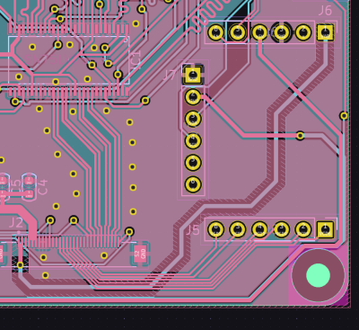
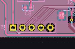
Then, let’s take a look at a less obvious but still very pertinent problem – is the pin 1 orientation of the connector correct? It’s one of the easiest mistakes to make, and I know that because I’ve made it a couple of times before I learned to be cautious. One potential failure factor is that we got this pinout from a schematic we miraculously found online, and we got the connector footprint from a different spot – there’s already two points at which someone could’ve reversed the pin 1 marking, and if they don’t cancel out, the resulting bodge will be ugly.
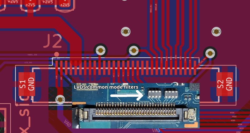
Thankfully, this one has a simple solution – comparing to the actual physical board we’re reverse-engineering. Here’s the real-life connector picture, next to our footprint in KiCad, and it speaks for itself. Now, if it had turned out to be the opposite, this picture would’ve been way funnier, but it’s also pretty good we have no mistake to fix, because rotating the connector could’ve been annoying mechanically. Oh, and we should probably include the LVDS common mode filters at some point – they’re not strictly required, so this revision is lazy with them, but they are nice to have.
Traces Are Cheap
Here’s some PCB design mindset advice I’ve figured out over the years, something that drives most of my PCB design decisions. Routing tracks and adding silkscreen text is cheap, making bodges is expensive. With this in mind, we take a look at the traces and the connectors – and there’s really only two connectors to keep in mind.
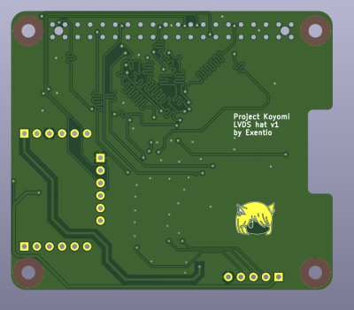
First of all, there’s the Raspberry Pi GPIO header. There are a few unused GPIO pins on it that are left un-utilized that we could easily fix. We’ve found that the unused pins happened to be default software I2C pins, and put them onto some pin headers – plus a JST-SH connector for QWIIC, again, this is very cheap to do. This is simple.
 Now, there’s a bigger problem – the display needs external backlight driving, remember? [Exentio]’s idea was to only tackle RGB to LVDS conversion in this revision, and I understand it very well – backlight drivers can be intimidating. However, that means the v1 boards will be quite limited in what they can do, and we would have to use v2 for actual backlight circuit experimentation, and then v3 if we need to make any changes to the backlight circuit – which is likely.
The problem is that neither of us has designed backlight drivers like that, so this is going to be new – we will make mistakes. A mistake, however, might just result in us having to remanufacture this particular board, move the RGB-LVDS driver and the connector to a new one or discard them, or spend money on new ones. Every forced iteration to a project requires you to spend extra time and money, and every iteration is a step where you might never complete the project. Let’s make sure this project is easy to complete.
Here is a trick that lets you cheat and give yourself extra time to figure out backlight driver options, not have to produce any more of the main board’s iterations than you really need to, not have to get rid of these boards, and make driver circuit development itself simple. Let’s make an impromtu daughterboard header for the backlight driver! We’ve found two possible drivers, one with PWM/EN control and one with extra I2C interface, and pulled out some more GPIO pins so that we can control the driver in software.
For the daughterboard, we’ve added 2.54 mm headers on a 2.54 mm grid. Neither the header nor the grid pitch is required to be 2.54 mm, but it’s probably the best thing you can do for yourself because this pitch will be the easiest to work with when developing. Then, pull all the needed signals onto these headers, without skipping any capabilities. I’ve also added both 5 V and 3.3 V rails, because one of our drivers needs 3.3 V as well as 5 V, so it’s good that the daughterboard for that won’t need to have a 3.3 V regulator too.
 After the backlight devboard header is done, there are still a few unconnected signals left, which shouldn’t be important, but they could be fun to poke at. Again, traces are cheap, bodges are expensive, so we can pull them onto a separate 5-pin 2.54 mm pin header. And add pinout markings, because silkscreen is cheap too. Also, I’ve added a keepout around one of the LCD driver traces – it’ll have up to 60 V on it, which is not really a voltage you need a keepout for, but I decided to be overly safe with it.
Finished, Published, Waiting For Orders
I’ve reviewed this board in a call, and was applying changes to it as we spoke. After we finished the review, I’ve zipped the project folder up and sent it back. Whenever you review someone’s board and apply some changes on your end, you should also make sure to send them back, it helps! Some people will use the project as sent back with your changes applied, and some people will want to re-apply your changes themselves – whether because they want to learn these things themselves through practicing, or because that’s the way they’re most comfortable, both are okay.
We finished this board a couple months ago, but we haven’t yet ordered it. It is ready to order, however, and we don’t need to figure out the backlight circuit before we do so, so all I need to do is to poke [Exentio] about it or order them myself! It is also a nice DPI-LVDS reference design for any Raspberry Pi hacker – the design is now public on GitHub for any of your copying needs. About the only thing left that would’ve been nice to add is series resistors for the DPI interface, but they’re not that crucial, and definitely not worth moving the traces around to add – I might add them myself whenever I move this chip to the Sony Vaio design.
This board is a start for the design review series, and it’s also the first building block into our Sony Vaio rebuild project. Speaking of that project, one of our chosen ICs has recently acquired Not Recommended For New Designs status, which means we must immediately use it to design a board!


“one of our chosen ICs has recently acquired Not Recommended For New Designs status, which means we must immediately use it to design a board!” ….. nice article, but not sure if this line was a joke or not (maybe use double or triple exclamation marks for jokes)
I think it was sarcasm, LOL.
Example: I like nothing more than using a component in a new design that they dont plan to make much longer!
Here is Gemini’s verdict: “Yes, the comment “one of our chosen ICs has recently acquired Not Recommended For New Designs status, which means we must immediately use it to design a board!” is most likely an example of sarcasm.
Here’s why:
Logical disconnect: The suggestion to prioritize an “Not Recommended For New Designs” component makes no practical sense.
Humor through exaggeration: The forced urgency (“must immediately”) emphasizes the absurdity of the situation.
This comment is likely a sarcastic way to express frustration with a situation where they may be forced to use an outdated component due to limitations or constraints.
Sources
hackaday.com/2024/03/12/design-review-dpi-lvds-sony-vai”
…. What is rather strange to me is that the Ai cites this very article, which was only published a few hours ago ….. unless it was able to hack into the Hackaday editing system or the author’s PC and see it some days ago.
yep! that said, it shouldn’t be that horrible to use it either – we wouldn’t need that many of these ICs or to use it long-term, and the daughterboard idea lets us have this IC as one of the (currently) two options for bringup!
I wasn’t sure either. Part of me says “get the design out quick” because you usually have a few years afterwards. But the other part of me has parts-shortage trauma, and thinks redesign now saves work later.
Is it a “new design” if you’re halfway done?
Good article, thanks, I love your down-to-earth practical articles.
But it would have been way better if a board had been made and tested before publication so we know if anything still managed to slip through despite review: sort of reviewing the review process.
Also having read all the above I’m a bit unclear still if the review process uncovered any actual mistakes that would have stopped the original design working. Improvements yes, but any actuall errors?
There were a few mistakes – selecting the wrong regulator and confusing 0603 metric and 0603 imperial.
Regulator /might/ have worked. Wrong footprint would have required another order from digikey with the right sized caps and a steadier soldering hand than expected, but likely wouldn’t have required a botch. Unlike making the same mistake for resistor arrays, for example, where it is more likely that the exact value and configuration isn’t actually available in the “wrong” size.
This board is a continuation of the Sony Vaio rebuild saga, so you will inevitably hear more about it ^~^
Great article and project.
One minor issue: check the clearance between board edge and copper. Recent versions of KiCad default to 0, which may lead to exposed copper on the edges of the circuit board.
Based on the images above, that also seems to be the case on this board.
ohh, true! it’s something I only started caring about recently, because manufacturers never complained and I never had issues, but you’re very much right!
This sounds like a great resource for Raspberry Pi hackers! Exciting to hear that the design is publicly available on GitHub. Looking forward to seeing how it evolves, especially with potential tweaks for the Sony Vaio design!