Usually, designing a CPU is a lengthy process, especially so if you’re making a new ISA too. This is something that can take months or even years before you first get code to run. But what if it wasn’t? What if one were to try to make a CPU as fast as humanly possible? That’s what I asked myself a couple weeks ago.

Stovepipe was made at break-neck speeds
Like I said earlier, Stovepipe’s hardware was finished after a mere 4 hours. Add another 2 total hours for the assembler I made afterwards, for a total of 6 including the programs, spread over one week. I estimate GR8CPU was originally designed in just over a year, including tooling, in occasional afternoons after school spent designing. That timespan is notably over 50 times longer than the week that Stovepipe was spread over. In a similar light, Boa³²’s minimum viable product (RV32I) was completed in almost exactly two months, or 8-ish weeks. Still, 8 times as long as Stovepipe took to make. I have no concrete numbers of course but I believe that the real time spent in hours to be even worse for both GR8CPU and Boa³²; almost certainly more than 50x and 8x the hours (so 300 and 48 at the very bare minimum) respectively. How is that possible?
Because it is a simple CPU
Part of it is, of course, experience. GR8CPU, which has appeared on Hackaday long before I was a writer, was my second ever microarchitecture and [Ben Eater] didn’t exactly start studying CPUs immediately after his YouTube series like I did. However, Stovepipe is also an exercise in minimalism; unlike both GR8CPU and [Ben Eater]’s, the only user-accessibe register is the accumulator and every calculation with a second operand has to deal with memory. It has 256 bytes of RAM, on par with GR8CPU, but no I/O ports of any kind; all I/O must be memory-mapped. Stovepipe instructions take 1 cycle to fetch and 1-3 to run (except NOP, which takes 0 cycles to run). On par with both GR8CPU and [Ben Eater]’s, it has a carry out flag and zero flag.
Compare this to my most recent previous CPU, Boa³² (a RISC-V implementation), which is larger by a seemingly extreme amount despite being only about as powerful as modern microcontrollers. It’s 32-bit, has 31 general-purpose registers, 3 of which are usually used for special purposes, a full 4GiB address space, 512KiB of which contains RAM, hardware multiply/divide and atomics, etc. And most importantly, is pipelined and has separate address and data busses, unlike Stovepipe, GR8CPU and [Ben Eater]’s, all of which are multi-cycle single-bus architectures with a dedicated address register.
But how does it perform?
Let’s compare two programs: Computing the fibonacci sequence and multiplying an 8-bit number; across three CPUs: Stovepipe, GR8CPU and Boa³². I will write it in assembly for all three, ignoring Boa³²’s hardware multiply to keep it fair. Let’s dust off the old projects for a short moment, shall we?
| CPU | Multiply set-up | Multiply loop | Fibonacci set-up | Fibonacci loop |
|---|---|---|---|---|
| GR8CPU | 27 | 22-38 | 24 | 40 |
| Boa³² | 2 | 7-8 | 3 | 8 |
| Stovepipe | 18 | 22-29 | 15 | 27 |
To my surprise, GR8CPU actually performs significantly worse than Stovepipe, mainly due to it needing 3 cycles to load an instruction compared to Stovepipe’s 1. On the other hand, to absolutely nobody’s surprise, Boa³² wipes the floor with both Stovepipe and GR8CPU because of its 32 registers and pipelined nature. It executes most instructions in a single cycle spread over its 5-stage pipeline.
Conclusion
Trying to speedrun making a CPU was clearly a success given the scope; in merely 4 total hours, I made a CPU that outperforms my old 8-bit CPU while being much smaller. The whole exercise shows that simpler is sometimes better, though not always, because the speed-optimized Boa³² easily beats the size-optimized Stovepipe in a landslide performance victory. Stovepipe, however, completely demolishes most CPUs I know in terms of size; [Ben Eater]’s, GR8CPU and better-known CPUs like the 8086, 6502, z80, etc. are all easily defeated by Stovepipe in this respect. That’s not a world record, though; I believe that [olofk]’s SERV CPU is smaller than Stovepipe, though I cannot make a direct comparison due to Stovepipe existing only in a logic simulator.
By the way: If I do ever do a Stovepipe 2, I’ll record the entire time with an actual speedrun timer ;)


FPGA?
I would say yes. Breadboarding even a simple CPU like this one on TTLs would definitely take more time.
Good, now make this CPU able to work in a parallel fashion.
The article reads like the CPU wasn’t implemented, which is fine, but the title reads like it was. Comparing cycle count for specific programs isnt super fair, as one could design a CISC CPU with arbitrarily long delay paths that would be either unroutahle or have arbitrarily slow clock speeds. I imagine this isn’t the case here due to stovepipe’s simplicity, but it would be great to see if it can place&route reasonably well.
Maybe there’ll be a follow-up article! I’d also love to see Olof’s SERV core thrown into the mix ;)
Stovepipe was made in Logisim, a digital logic simulator by cburch. I have no plans to port Stovepipe to Verilog nor do I have plans to build it out of TTL because those are for a new (non-speedrun) size-optimized CPU called Faerie.
You could just import it from logisim into logisim-evolution or digital and then export it in verilog.
It looks like it’s simple enough to fit into a CPLD, like one of the Philips CoolRunner line. These have the advantage of being single-chip, and they don’t have to be loaded from an external EEPROM every time they are started up.
..and this actually COULD be built in a very short time, as hardware.
okay, cool, no doubtm seriously, I like these kind of project (fast or slow).
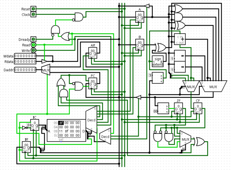
But “Stovepipe’s hardware was made in under 4 hours” and no pictures… I’d like to see some pictures or is there no physical hardware, if so then I’m confused. I assume this is the first article in a series?
Please tell us more…
My bad, I added a screenshot of it for you ;)
Soooo…. “Stovepipes hardware was DESIGNED in 4 hours.”
Don’t get me wrong, this is really cool and well beyond anything I could ever hope to achieve. But I have to agree with the other commenters, the article title and some of the bits in it make it sound like you were physically making this. It was not clear that this is all just being simulated.
Which means the CPU logic was designed.
Logisim can’t simulate electrical components so no hardware. No hate on the CPU, just more at logisim, and more yet how people so confuse its use.
No tri-state, no latency, no voltage/current.
“logic” slots into maths right next to “arithmetic”, making logisim an advanced visual calculator of sorts.
Ok, now synthesize it, let me know what frequency it can run at, and it’s performance relative to something else for some basic benchmarks.
It’s just another paper cpu.
When done, will you write a DOS for it?
ADA compiler?
B^)
Picking of a nit: according to my Ada instructor a quarter-century ago, ADA is the American Dental Association.
As a cotton picking nit picker my self, I stand corrected!
B^)
“Microsoft purchased 86-DOS, allegedly for US$50,000.”
Surely you mean will Bill pay $50k to someone ?
Tiny Tapeout Time!
Once this process can be made fast, it is time to add a genetic algorithm with lots of mutations and really crank it up a notch, after a few billion generations we will have earth 2.0 :) (with or without fjords creating the African coast, not everyone is like Slartibartfast and enjoys a lovely baroque feel to a continent).
I will wait for Earth 42.0
hah i wish i hadn’t read the comments because i was imagining building a cpu in an afternoon. i would probably go for an eeprom (microcode consisting of enable lines for the register latches), a handful of 8 bit latches, and an sram. i think i have those handy in my basement….but i don’t know if my eeprom programmer still works so maybe i’d use a pico to provide usb-addressable eeprom :). and initial program load is kind of a challenge – maybe the pico can take over the bus for a moment to program the sram before starting up the clock! hah.
i’ve done some bulk wire-wrapping before so i think i could do all the connections for that in an afternoon. you know, it might even fit on a breadboard…probably stay up half the night getting the microcode just right.
just kind of a different question whether you’re trying to minimize design complexity or minimize implementation complexity.
simulation never = reality. Put it in silicon and see if it’s as good as you rate it. This exact issue has been covered by youtuber Dr plague.
This is a simple enough CPU, that if you get the logic right and it survives simulation, it’s almost guaranteed to work in hardware, especially if implemented in a CPLD. In their day, these were a lot less fussy than FPGAs.
[Ben Eater]’s 8-bit computer was a project intended as an instruction tool, illustrating what each chip (or macrocell, or circuit block) in a CPU does, and why. The series of videos that describe it are the most clear and concise explanation I’ve ever seen of a CPU. If you wanted to speedrun it in a fair contest, you would need to create a set of YouTube videos that show every step of the process of designing and building it. Otherwise this is pure apples and oranges. [Ben] even points out that his CPU is not suited to actual use for anything due to its extremely limited memory address space, and his subsequent projects are all 6502-based. It’s a little bit hand-wavey, but the point is that if you can understand his CPU, you understand everything that goes on in a 6502, but it would just be silly to try to go any further with his CPU than blinking LEDs and simple arithmetic demonstrations.
Damn, beat my time of 8 hours. I did the same half a year ago in Verilog. 8-bit RISC-V inspired CPU, but also included time spent writing verification test cases and peripherals in the timer, as well as flow runs (no “load remover”, you could say). Maybe I need to have another shot at it.
Oh, and I thought this post is about Intel …
;)
Maybe it’s time to plug my 4-bit “CPU1” which I also designed in a matter of a few hours, while on holiday in Japan, and during a discussion where I tried to convince someone how easy it is to design a CPU from scratch.
https://imgur.com/a/WWdIzO5
While I rewrote this, because of a couple “invalid token” errors I forgot to include some information. So here’s that information and even more of that information.
256 bytes ROM, 8-bit instructions, Almost completely orthogonal IS (each bit in the instruction has a meaning that is from the others, and there’s some ), 4 bit data path, ALU has only two operations (add and NAND), ALU Input1 is literal, mem, or zero, ALU input2 is “register” or 0xF, Relative short jump and absolute far jump, Jump to 0xFF to break (different from halt), Separate display driver (text-mode “video card” outputting serial ASCII (bin2hex for “register” input)), , No thoughts were spent on making this compatible with higher data-bus widths, Designed in 2012 in the original Logisim. Text in the screenshot looks cramped because it’s not HiDPI compatible.