Until the late 1990s, the concept of a 3D accelerator card was something generally associated with high-end workstations. Video games and kin would run happily on the CPU in one’s desktop system, with later extensions like MMX, 3DNow!, and SSE providing a significant performance boost for games that supported them. As 3D accelerator cards (colloquially called graphics processing units, or GPUs) became prevalent, they took over almost all SIMD vector tasks, but one thing that they’re not good at is being a general-purpose parallel computer. This really ticked [Raph Levien] off and it inspired him to cover his grievances.
Although the interaction between CPUs and GPUs has become tighter over the decades, with PCIe in particular being a big improvement over AGP and PCI, GPUs are still terrible at running arbitrary computing tasks, and even PCIe links are still glacial compared to communication within the GPU and CPU dies. With the introduction of asynchronous graphic APIs this divide became even more intense. [Raph]’s proposal is to invert this relationship.
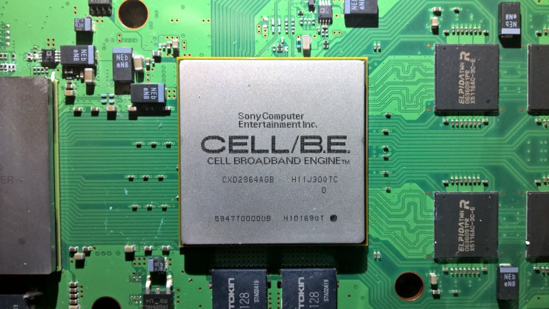
There’s precedent for this already, with Intel’s Larrabee and IBM’s Cell processor merging CPU and GPU characteristics on a single die, though both struggled with developing for such a new kind of architecture. Sony’s PlayStation 3 was forced to add a GPU due to these issues. There is also the DirectStorage API in DirectX, which bypasses the CPU when loading assets from storage, effectively adding CPU features to GPUs.
As [Raph] notes, so-called AI accelerators also have these characteristics, with often multiple SIMD-capable, CPU-like cores. Maybe the future is Cell after all.


The Super Nintendo had used co-processors in early 90s already.
Or “Mappers” in NES or Gameboy terminology.
SuperFX chip might be most popular, but there also had been 6502 derivatives (or 65C816 derivatives rather) doing the work of the main processor.
https://en.wikipedia.org/wiki/List_of_Super_NES_enhancement_chips
Mappers aren’t coprocessors.
There were additional CPUs on snes and genesis because technology moved faster than the console life cycle. However they generally took over from the main CPU.
The Amiga copper is probably the earliest home example of a coprocessor. The dsp on the Saturn is where things got kinda interesting
No, the BBC Micro had a full co-processor architecture via its Tube interface, a few years before the Amiga was released. This supported plug in coprocessors, including a 2nd 6502, and also a z80 board. No custom gfx coprocessors as far as i recall, but the 3D game Elite had an enhanced version that leveraged the 2nd 6502 for gfx offload.
Not an apples to apples example, but as clise as it got to a gfx coprocessor in the early/mid 1980’s.
I’ve always been baffled by the RAM extension (whatever it was called the red module) for N64.
Was there really a period of time that 4MB of RAM was more expensive than adding the option to add 4MB?! The case complexity with a removable panel, the extra routing in the PCB, the termination module… Surreal!
Then by the time DK game was released the 4MB was a free pack in!
The RAM upgrade is RDRAM (Rambus RAM) which was expensive at the time compared to other RAM.
Ram used to be one of the single most expensive things on a console. The Xbox has 64mb total. It wasn’t till Xbox 360 and PS3 era memory became cheaper.
it helps to remember the context of the time, it was designed from the get go to do so, because the RAM expansion was expected to be used by the 64DD as primarily buffer space and for actual applications, which was not shipped for another 3 years after the N64 release. the 64DD failed, but they had manufactured a boatload of the memory paks, so developers added support to a lot of games and nintendo encouraged them to liquidate their stockpile, the games that needed it would pack it in.
Ah I did not know that!
“Until the late 1990s, the concept of a 3D accelerator card was something generally associated with high-end workstations.
Video games and kin would run happily on the CPU in one’s desktop system, with later extensions like MMX, 3DNow!, SSE, etc.
providing a significant performance boost for games that supported it.”
That’s true, I remember the MMX being hyped at the time Windows 98 was new.
It was neat, because it was mapped on the existing x87 registers.
Seems like a waste, but it solved an issue: context-switching.
Many older multitasking environments such as Windows 3.x did save/restore x87 status when multiple applications were running and trying to use math co-processor.
So sharing the math co-processor didn’t cause a mess.
MMX registers mapped on x87 registers were saved/restore same way, so MMX could be used in such environments without any changes.
(SSE could be used by applications under older single-tasking systems such as DOS, too.)
Back when MMX was new, there had been visions of MMX replacing 3D accelerators and modems.
MMX was being considered to implement software-based DSPs, which could do a lot of things. High-speed modems, voice recognition, 3D sound, rendering, virtual reality etc.
Photoshop and other drawing programs used MMX optimized filters.
The positive side was that the processor doing 3D calculations had fast access to caches and main memory,
while 3D accelerators such as 3dfx Voodoo or NEC PowerVR had to hog the PCI bus.
Data had to be copied between main memory and graphics memory, slowing things down.
Unfortunately, MMX was integer and could have had benefited greatly by working in tandem with something like an x87 FPU (80×87 was also capable of integer math btw).
AMD’s 3DNow! Instructions sorta combined the strenghts of both MMX and x87 FPU on top of the old math co-processor registers, but wasn’t adopted by intel (VIA oder Cyrix did adopt 3DNow!).
Btw, also interesting were so-called “Transputer” cards for parallel processing.
They had their own memory and processor and were being programmed by the host system.
LISP systems had been built on Transputer technology, too, I think.
That’s interesting insofar, because LISP used to be related to A.I. (things like neural nets, expert systems etc).
Transputer was both a series of inMOS processors (T800 etc), as well as a concept, I think.
https://en.wikipedia.org/wiki/Transputer
https://www.abortretry.fail/p/inmos-and-the-transputer
The Transputer! I have two ISA Transputer boards I dumpster-dived from a college in southern Ohio in the 1990s, and I even got one of them to work using code I downloaded circa 2002. Researching Transputers successfully (using InfoSeek, as I recall) was the first proof-of-concept I had that the Web was going to be a very useful tool.
I worked as a maintenance technician at the Inmos USA facilities for most of the 1980s. First in final test (Teradyne and Pacific Western (Colt) testers. MCT, Thermonics and Symtec handlers) and later Probe (EG probers, Teradyne testers and fuse blowing lasers).
The original RAM fab was at the Harrison (office) park facility while the new fab (on “the hill” as we called it) was under construction/completion. It would later be used for process development until decommissioned around 1985 I think. Final Test/burn in was at Harrison Park, Probe on “the hill” with design and fab. I can’t remember where assembly was.
The transputer was often touted (often by Mr. Barron himself) as the future of the company. The butterfly demo video in the AbortRetry article video was first presented to us on two monitors with the butterfly flying between the two to show off the power of parallel computing. Greeted by many ooohs and aaaahhs.
We in the US saw little of the transputer though some of the transputer boxes did flow through our world. During a recent move I found a couple of massive T800s with technical and Occam docs. I wonder if they are worth anything?
As an underling, I never knew of or experienced conflict between Wales and us. Being young and single I often took the visiting UK techs and engineers out on the town after shift. A couple of times joined by Barron at his 4 Seasons hotel bar or The Pelican Club. He wasn’t above tipping a pint with us.
Those were heady days!
I’d still be interested in seeing some CPUs that are basically restricted to single cycle operations or even more limited but tons of them and then use special compilers and threading tools to spread operations across cores.
That’s kind of how VLIW architectures like the Itanium and Transmeta Crusoe worked.
One big challenge that inhibits GPU’s from being used for general CPU tasks is context switching. A massively SIMD architecture carries huge ammounts (thousands of ALUs with dozens of registers each) of state, which simply doesn’t lend itself to the fine-grained load/restore needed for a multi-process OS. Local memory exacerbates the problem since it’s also a limited resource, and would need shuffling around much more often if you try to context switch at the rate needed for general tasks.
If you had enough nodes, you could just run everything continuously in parallel, adjusting the nodes per task rather than switching context.
I remember when the CELL processor came out. The architecture was interesting and I wanted to write some neural net bits to take advantage of the parallelism.
Add that to the list of projects I never got around to.
I had the misfortune of having to write for the CELL, and it was awful. Such a finicky architecture that really wasn’t fast enough to justify it’s BS. I ended up having to write my own task manager/dispatcher for the SPUs, which was interesting and the basis for my PhD thesis work, but still sucked ass. And, that’s not even discussing the awful tools that IBM provided to do development.
I miss the Parallella/Epiphany and the Xeon Phi.
I still have two Parallella boards. Mainly for experimenting with the Xilinx FPGA, not so much for the Parallella itself.
I would just like to point out that many CPU packages use PCIe links internally, so that sentence is a bit confusing.
Not sure how to fix it, maybe say PCIe slots? That makes it clear what you are referring to without getting into output logic design vs on die or on package PCIe links.
(I haven’t found much to read on the subject, I just notice that most Ryzen APUs only get 8 lanes for PEG cards (PCI Express Graphics). Yet the Ryzen 5700G for example has a x16 Gen3 link. Meanwhile the integrated GPU claims x16 links on newer Ryzen 7700 with integrated GPU.
I remain curious as to the internal layout.
AMD’s older APU’s have 16x PCIe lanes total which gets split up into 4x lanes to the chipset, 4x lanes to a dedicated NVME SSD (usually the top M.2 slot), and 8x lanes to the primary PCIe slot for a GPU. That’s all 16x lanes used up right there. 🤷
Once i learned about the holographic processor that microsoft designed for the hololens 2 dev ed that I have. Ground up design and custom architecture. Check that out if you want to see some co processing that actually works well together. It supposedly handles all the dedicated graphics in and out while leaving the processor free to compute only what it has to as far as programs go. I think i remember reading that it took nearly 20 years to develop the chip, language, software etc.
put my finger on how i read this article twice without finding any meaning in it
headline says ‘a good parallel computer’, body says ‘GPUs are still terrible at running arbitrary computing tasks’. imo for the kind of inherently parallel tasks that GPUs are used for, they’re pretty good. and they’re progressing. for arbitrary non-parallel (one of the comments mentioned ‘task switching’!! parallel’s opposite!) tasks of course they aren’t used.
you have to decide what your task is before making something good for that task, but this article can’t decide what it’s criticizing.
shrug
The TI 990 series of minicomputers and the TMS9900 microprocesor implemented registers in a block of memory with a pointer to it in the CPU. Context switching was done by simply changing th pointer. I believe the TI 990-12 and 990-15 implemented the first several KB of memory with fast static RAM. It ran at register access speed. The family never made it to 32 bits because TI decided it could make more money with less investment by selling semiconductors then selling minicomputers. RIP.
The fact that Sony added a gpu to overcome cell limitations it’s absolutely false informations I don’t know where do you find such stories
The Cell was not meant to be used as gpu I don’t know where you found such false story
I’m surprised we haven’t seen a GPU with a typical GPU primary chip but with an arm cpu on card and most importantly on the same memory bus. It’s not perfect, but it would make gpus more capable parallel compute wise.
Ultimately having dedicated centers for compute tasks is the limiting factor. Having a true APU with chiplets for processing, cache, sdram, NV storage, gpu/npu, etc is going to be needed along with a good software layer to leverage it. Doing that sounds nice but then your start getting into limits in thermal and power density in the physical chip. Computers are hard.
Hololens 2 did that exactly. And well.