[Editor’s note: The hacker requested that we remove the image for legal reasons, so it’s blurry now. We hope all’s well!]
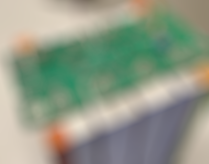
Lithium technology has ushered in a new era of batteries with exceptionally high energy density for a reasonably low cost. This has made a lot possible that would have been unheard of even 20 years ago such as electric cars, or laptops that can run all day on a single charge. But like anything there are tradeoffs to using these batteries. They are much more complex to use than something like a lead acid battery, generally requiring a battery management system (BMS) to keep the cells in tip-top shape. Generally these are standalone systems but [CallMeC] integrated this one into the buswork for a battery pack instead.
The BMS is generally intended to make sure that slight chemical imbalances in the battery cells don’t cause the pack to wear out prematurely. They do this by maintaining an electrical connection to each cell in the battery so they can charge them individually when needed, making sure that they are all balanced with each other. This BMS has all of these connections printed onto a PCB, but also included with the PCB is the high-power bus that would normally be taken care of by bus bar or nickel strips. This reduces the complexity of assembling the battery and ensures that any time it’s hooked up to a number of cells, the BMS is instantly ready to go.
Although this specific build is meant for fairly large lithium iron phosphate batteries, this type of design could go a long way towards making quick battery packs out of cells of any type of battery chemistry that typically need a BMS system, from larger 18650 packs or perhaps even larger cells like those out of a Nissan Leaf.


I woukd to see this for 18650.
A Pcb bms to plug the battery directly for 4s or more
Hi !
Thanks for the suggestion, I think it has been made by other people in the past, but I’ll give it a look.
For 18650s you’d need a clamping force directed along the long side of the cells.
Take a 2S2P pack.
Two square PCBs and they have 5 holes, 4 in each corner and one in the centre.
However these are also soldered onto the board and you pass threaded metal bars, 5 of them, through the top holes and into the bottom holes.
And because their nuts are soldered onto the board they act as individual conductors to let the charging circuit and BMS charge the cells individually.
So, Cell1 Positive directly touches the board at the top plate position 1+.
Cell1 Negative directly touches the bottom board in Position 1-.
1- has a trace to Bar1 and Cell1+ and Bar1- are connected to Cell Position 1 on the BMS IC.
Repeat 3 more times and you have a BMS IC with direct connections to Cell Positions 1 through 4 in the BMS IC.
Why did you delete your repo? I was very interested in this.
Looks like they are facing licensing/copyright issues and temporarily made it private.
https://github.com/EagleOne42/unifi_video_ir_control/issues/6#issue-2961283869
Wow … I need exactly this! I’m sitting on 8 EVE cells that I’d like to turn into a couple of 12V batteries, I checked out the GitHub page but can’t tell if the creator has plans to sell these?
It looks like all of the files you need are there to send it off to a fab like jlcpcb and have the boards made. You could even have them assembled if you don’t want to solder the SMD parts.
Hi !
Since there are still few adjustements to make it Plug&Play I do not sell those yet, maybe in the future. In the meantime, fabrication files are availiable as well as software :) Enjoy!
With those large cells I’d be concerned of normal and in-use thermal expansion/shrinking stressing the PCB.
AFAIK proper packs with those dimensions use (heavy gauge) copper bridges that are either flexible or at least with decent hump/bend in it…
And the “external” +/- pole holes seem to overlap with the cell below – looks to me like fitting a screw with nut/washer in/through there might be a tad difficult.
Look closer – the cells aren’t butted up against each other, there’s a cardboard spacer between each pair. That should be plenty of room to accommodate any pack expansion without putting stress on the PCB.
Manufacturer datasheet recommends 3kN (300kgf) compression force for these cells. Though people often assemble prismatic cells without compression. With fast charge/discharge that will eventually result in significant swelling, way more than the few millimeters from the cardboard. But then again, looks like the manufacturer is selling brackets that give no compression at all and similar few millimeters of spacing.
Hi!
Yes you’re absolutely right, these cells tend to swell under load, this picture is more of a fast POC, I’m working on mechanical brackets to hold the cells. Thanks for your feedback!
Oh I saw that – cardboard?! no please don’t.
But even disregarding the fact it’s highly flammable wood – what about the other relevant expansion axis?
You can get LFP cells in that form factor that you wouldn’t need to worry about thermal runaway as much with
Same here, also the large ceramic resistors sitting right on the small bridge of PCB material are just asking to get cracked by even the slightest twist or movement in the PCB.
It’s a nice concept but needs a little finessing from a mechanical perspective.
I don’t see MOSFETs anywhere to cut off charge/discharge. Without those this could potentially be quite unsafe.
Yeah, looks like this only does monitoring & balancing and not protection. The PCB tracks will fuse at some point, but with 6W dissipated per link, the 200 A continuous rating does not seem impossible.
The C6 & C7 ceramic caps across the whole battery seem a bit scary too. If they short out due to mechanical damage, it could result in a nice arc fault that might not self-extinguish.
The README explicitly states it’s intended to be used with an external relay and it includes an output to drive it.
Battery charger
Hi!
You are right, because of the high currents, I didn’t plan on using a MOSFET, however, there is an open-drain output with flyback diode which can be used to drive a power relay (TE Conn has some high current DC Relay). I will try to add a MOSFET in the next (hopefully final) revision of this board.
A MOSFET only blocks current in one direction, so you need two to protect both directions. Multiple MOSFETs will be needed in parallel to handle the current. They have to survive a short circuit long enough for the BMS to shut them off. The 100A BMS that I have uses 10 TO-263 MOSFETS in parallel, the bigger ones have a lot more.
Those large 4R7 resistors placed above the PCB constrictions will be disproportionately susceptible to termination and solder joint failure.
If they really have to be there, split them up into 2-4 small ones in parallel, with their long axis oriented perpendicular to the axis of the bridge.
There is no reason for any PCB cuts. It’s no a HV circuit. And extra PCB thickness would make sense
It’s the first thing I’ve seen too! Here to write it down but you were faster ;) Anyway it’s not a bad idea!
Hi! Yes that’s true, thanks for your feedback! I will split them and move them to a better location.
regarding my mechanical criticism above:
What if instead of connecting the PCB directly to the batteries you kinda “float” it above and make every pcb2cell connection via a C-shaped flexible copper strip thingy (dunno how to call them)
https://duckduckgo.com/?q=high+power+flexible+copper+lithium+u-shape+strip&t=ftsa&iar=images&iax=images&ia=images
I was drawn to that too, they are really begging to get cracked by any flexing that happens in that position.
Given the type of cells and the anticipated current levels, proper electrical connectors are necessary. Although PCBs may work initially, they are not designed to provide the mechanical robustness and long-term reliability required in such applications.
Hi! That is true indeed, I think some pressfit connectors from Wurth could help! As well as proper mechanical structure arround the pack :)
I’ve done 60MWH projects for IBM. Torqued all the busbar down, coated all the plating. PCB does not like the torque necessary to ensure a large surface area electrical connection can go through a hundred thousand heating cooling cycles before being retorqued. While there was mention of thermal expansion, the other problem with a delta T is condensation, which in this style design would develop on the underside of the links, causing tracing right past your bms, or worse if it drops down to a rack below. Copper, tin, nickel, silver, all have much more similar coefficients and expansions. PCB is more thermally like bakelite, especially when it is thick enough to have 600V and 1000A on it.
That’s impressive !
Thanks for the feedback :)
Though nice in concept, the copper on the pcba certainly dont have the mm2 to support the currents these cells can support. (200A sustained).
In battery packs nowadays they have flexibele busbars to connect these cells to support the shrinking and expansion of the charging/ discharging. This fixed connection would give a lot of stress to pcba/ battery pins.
Hi! The 200A were sustained for a few minutes, unfortunately I don’t have a load capable of sinking 200A for more than few minutes. I tried to jumpstart a combine harvester which sinked about 400A for couple seconds.But it would be a good idea to add complementary busbars if needed.
This project aims at reducing pack manufacturing complexity, especially by removing the need of solder or external wiring :)
I added “improving PCB shape / structure” to my To-Do list, maybe using FPC might help!
Why does it have a serial console?
Hi! At the begining of the project, CAN Bus was not implemented, hence the serial console for easy debuging.
Just checked the Gerber, looks like the separation between the ground copper pour and the pack + terminal area is only 0.3mm. Not sure if this is an oversight? It’s probably safe voltage-wise, but why have giant gaps for connections at lower voltages then? Also can anyone tell me how it manages individual cell charge/discharge? It looks like there’s only a couple of AO3400A’s that bypasses charging current through a resistor, I guess that counts?
Hi! You have sharp eye, indeed that is a mistake, I will definitely improve this in the future.
The individual cell discharge is handled by optocoupler driving N-MOS to discharge the cell in a resistor.
The balancing phase is started close to the EOC (90% SoC if I’m right). Since these packs have fairly large capacity, it is only needed to balance the system once after manufacturing (which might take a while!) and thanks to the auto-wakeup system, the packs balances itself and maintains uniform cell voltage. This feature lacks documentation, I will update it shortly. Thanks again !
Did CallMeC remove the github repo? The link no longer works.
Looks like a different – but similar – project? The photos show a different PCB (rounded busbars)?
I really like the project, hope the github comes back online!
This is a BAD IDEA! Cells wiggle around a lot over their lives. Heating and cooling and expanding and contracting will put enormous pressure on the cell terminals. You want to avoid that at all costs; not only does it stress the terminal seals, but also causes your bolted high-current connection to move around which isn’t good for long term resistance integrity.
Toyota learned this the hard way on all their hybrids. They used a flat copper busbar and it eventually destroys the seal on the terminal and lets electrolyte leak out, which of course leaks out ON the friggin’ bus bar and sense wires!
Tesla famously connects the cell terminals to the busbar with small flexible bond wires that impart absolutely no stress on the cell.
In the case of those PCBs, it’s going to either put a lot of stress on the terminals, or the PCB, or both, and in addition; It’s also not a good idea to through-bolt PCBs with large fasteners; the PCB connection will relax over time as it gets permanently compressed, and reduce the contact pressure, and also allow oxygen into the joint. It’s a recipe for disaster if you are carrying high currents. At a minimum; There should be a “T” bushing soldered into the PCB that basically acts like a device to prevent crushing, but this will probably fail as the solder cracks.
Ideally you want to use a flexible busbar with a center relief, Something like this (no affiliation): https://www.18650batterystore.com/products/flexible-busbar-screws-and-nuts-for-eve-lf280k-set-of-4
Then run flexible wires (high strand count) with crimp terminals or kapton flex or similar from the busbar to your BMS for sensing/balancing.
If you need to terminate I high-current connection to a PCB, use one of the press-in bosses, such as the awesome Würth “Redcube” (search for it). Again, Tesla makes great use of these in a lot of their PCBAs needing very reliable high-current terminations that won’t fail in harsh automotive environments.
Yes; Elon is an A**hole, but Tesla has some of the best Engineering around, despite him!
I have a YoutTube channel where I explain a lot of this amazing engineering. (linked)