Most of us learned to design circuits with schematics. But if you get to a certain level of complexity, schematics are a pain. Modern designers — especially for digital circuits — prefer to use some kind of hardware description language.
There are a few options to do similar things with PCB layout, including tscircuit. There’s a walk-through for using it to create an LED matrix and you can even try it out online, if you like. If you’re more of a visual learner, there’s also an introductory video you can watch below.
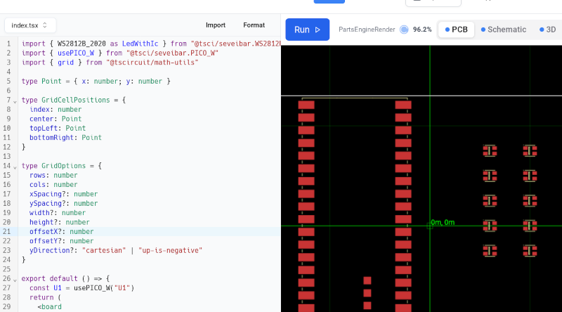
The example project imports a Pico microcontroller and some smart LEDs. They do appear graphically, but you don’t have to deal with them graphically. You write “code” to manage the connections. For example:
<trace from={".LED1 .GND"} to="net.GND" />
If that looks like HTML to you, you aren’t wrong. Once you have the schematic, you can do the same kind of thing to lay out the PCB using footprints. If you want to play with the actual design, you can load it in your browser and make changes. You’ll note that at the top right, there are buttons that let you view the schematic, the board, a 3D render of the board, a BOM, an assembly drawing, and several other types of output.
Will we use this? We don’t know. Years ago, designers resisted using HDLs for FPGAs, but the bigger FPGAs get, the fewer people want to deal with page after page of schematics. Maybe a better question is: Will you use this? Let us know in the comments.
This isn’t a new idea, of course. Time will tell which HDLs will survive and which will whither.


I dunno gotten pretty lazy with altium netlables and copy paste special for simpler repetitive things like the keyboard example … pretty sure ki-cad can do some similar magic tricks. For complex items maybe if you are a coder first, but since I have been doing ecad for over a decade now professionally not sure I could use a HDL and have it generate it for me any faster than just laying it out by hand (schematic or PCB)
I feel like I’d rather have an EDA tool be able to import an HDL rather than using the HDL as the base.
It’s different with an FPGA or ASIC because the HDL is doing two things at once – it’s allowing you to describe connections/entities and it’s allowing you to abstract the logic (you describe behavior rather than the bare entities). For cases where you’re just connecting things a lot of FPGA tools push you back to schematic-type objects (block diagrams, the bane of my existence, sigh).
But with a circuit schematic, what’s on the PCB isn’t a synthesis of what’s in the schematic, it’s supposed to be what is in the schematic.
In Kicad you can use python to manipulate components. Nets too i think.
it bring to my mind LTSpice.
It is essentially just a spice netlist, which is how some schematics are stored internally in simulators or schematic editors.
It seems like it’s putting a LOT of reliance on autorouting though, which is really not a very well baked technology. Doubly so for situations where RF considerations matter, even in the case of high speed digital signalling between chips and in power supply design.
There are a few boards that put caps near to chips but then stupidly connect them through vias and it’s possible this is due to an early autorouter going mad.
Autorouters have improved massively over the past 30 years, however they are still not good enough for real life designs. They only really work on the demo boards. I have rarely been given enough board space for the autorouter to work, and even that case, it is just faster to do the layout myself as setting up all the constraints for it to work still takes longer.
Years ago (>20) I was leading a team designing an ROV control system from scratch.
It was all done via descriptors not unlike these. From circuit boards to final wiring.
It was quite a project, some 24 months IIRC.
Many years ago I met MIT’s Prof Gershenfeld and he was experimenting with this concept. When I expressed doubt he gave exactly the same example: “You use HDL for big designs in an FPGA, why not for schematics and PCBs”.
Well – because in FPGA / ASIC the underlying structure is very uniform – it’s a lot of the same things from which the tools are building your thing. Schematics and PCBs are way less uniform – many different packages, lot of different rules. Analog ICs are also still designed mostly by hand – not enough structure.
So if you want boards full of 74xx logic, than HDL may work rather well, but anything more “analog” is a problem.
Even then, FPGAs are designed to eliminate most if not all analog concerns. It’s all converted into simple, generic numbers like the maximum fanout, so that analog stuff doesn’t need to be considered/computed at every junction.
You link to the atopile post at the end; coincidentally they’ve posted a few more feature videos recently https://www.youtube.com/@atopile_io/videos
I have just used Verilog in the past to design board level schematics.
Discrete chips and all named devices are just modules instances.
Wires are well, wires.
Many board level schematic tools can produce Verilog netlists as well, for simulation.
There are even tools that can take a verilog netlist a create well, a graphical schematic.
Not rocket science.
“Wires are well, wires.”
But not all wires are created equal. Especially in the analog domain.
Going from board layout to netlist rips away a lot of details. Putting it back requires detailed knowledge of design techniques. There’s a reason my copy of the black magic handbook is as thick as it is.
I am not laying out anything complex enough to justify the headache of learning and debugging an HDL project. And I would much rather use a schematic to troubleshoot a circuit than look at a mess of code and try to figure out where the signals all go.
Sue me, I am old school.
” Sue me, I am old school. ” Old school was the best school, and i agree with you 100%.
I can see the attraction of something like Openscad for PCB design.
Why not build it as a kicad plugin
Isn’t this already more or less what a .kicad_pcb file looks like in a text editor?
Were it built as a kicad plugin it would at the very least mean finding out about all the pesky analog concerns in board layout a lot faster.
Correct me if im wrong but isnt this pretty much an autorouter
Isn’t this how EDM is supposed to work? First capture the net list in the design, then lay it out on a board and have it auto-route or check your work using the netlist?
A lot of the time it’s easier to draw what you want than try to describe it in code. Describing it in code implies that you can generalize all the drawings into something simpler, and let the computer handle the details. In this case, it can’t. It would be a hard uphill battle trying to encode all the fun little analog rules of thumb people use every day, and design an optimizer than can solve for all these different constraints simultaneously.
Hello everyone! I’m the lead maintainer for tscircuit (the guy in the video)! Was delighted to see this on Hackaday, thank you!
To address some concerns in the comments:
1. We designed tscircuit to be somewhat reliant on decent autorouting. We’re betting on autorouters getting better rapidly, and we even develop our own autorouter which we believe will become state-of-the-art for open-source autorouting soon!
2. tscircuit is a lot more than a netlist! We can encode layout constraints, functional/simulation parameters and even information that helps to generate a Bill of Materials! We care a lot about making tscircuit a comprehensive and user-extensible spec. Again, there are lots of bets on future technologies like auto-placement and BOM APIs
3. Yes it is annoying to learn an HDL! I think that AI will help people to quickly onboard and also convert existing designs to tscircuit. The power is in having the specification aligned with your design intent, not necessarily writing it directly!