We’ve all made a few bad PCBs in our time. Sometimes they’re recoverable, and a few bodge wires will make ’em good. Sometimes they’re too far gone and we have to start again. But what if you could take an existing PCB, make a few mods, and turn it into the one you really want? That’s what “PCB Renewal” aims to do, as per the research paper from [Huaishu Peng] and the research group at the University of Maryland.
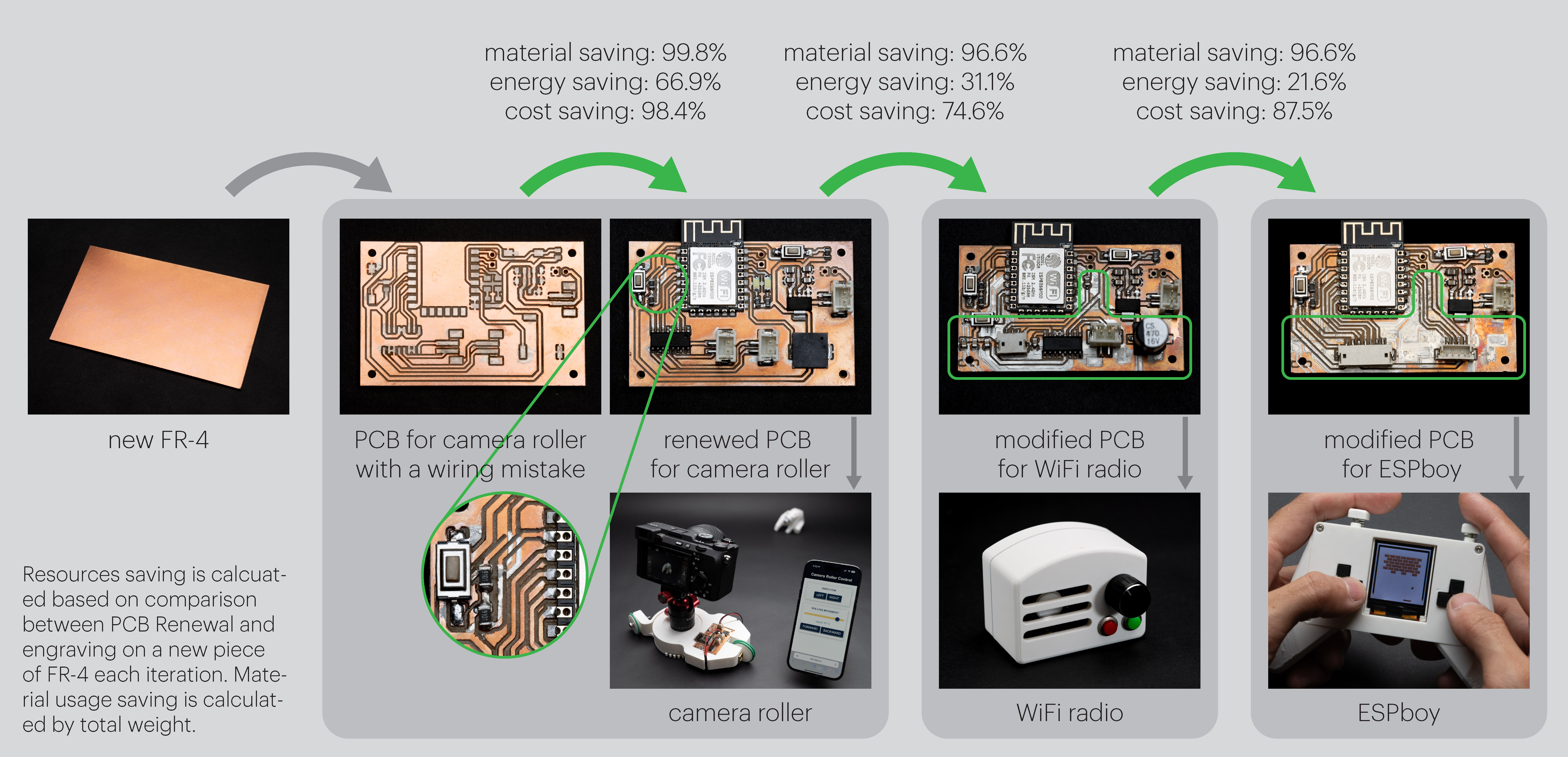
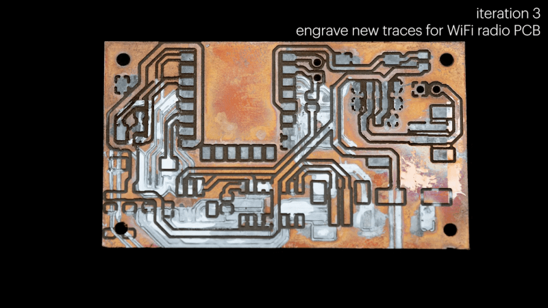
The concept is straightforward — PCB Renewal exists as a KiCad plugin that can analyze the differences between the PCB you have and the one you really want. Assuming they’re similar enough, it will generate toolpaths to modify the board with milling and epoxy deposition to create the traces you need out of the board you already have.
Obviously, there are limitations. You’ll never turn a PlayStation motherboard into something you could drop into an Xbox with a tool like this. Instead, it’s more about gradual modifications. Say you need to correct a couple of misplaced traces or missing grounds, or you want to swap one microcontroller for a similar unit on your existing board. Rather than making brand new PCBs, you could modify the ones you already have.
Of course, it’s worth noting that if you already have the hardware to do epoxy deposition and milling, you could probably just make new PCBs whenever you need them. However, PCB Renewal lets you save resources by not manufacturing new boards when you don’t have to.
We’ve seen work from [Huaishu Peng]’s research group before, too, in the form of an innovative “solderless PCB”.


Good job to Zeyu & Advait, cool seeing our lab being featured on one of my favorite websites :)
I’m sorry but this is just silly
This might be useful in some highly specific situations but in general putting effort into modifying PCBs isn’t work it. However, if the deposition machine can be miniaturized then it might be useful for modifying a PCB for espionage reasons.
There’s literally an entire industry out there that disagrees with you.
Getting PCBs reworked is surprisingly cheap: I screwed up an FPGA design that required removing a BGA, cutting a trace, and wiring a new trace to a previously unconnected pad.
Got a quote for it. About $300/board in single qty. Way, way cheaper than another assembly run.
Just depends. I’ve probably done some small amount of ECOs on every board I’ve done over the past year, just because I’ve been overloaded and fixing small stuff is faster than making sure everything is perfect.
I am finding it really hard to come up with situations where this might be useful. Maybe a useful research direction would be to look into improved ways to recycle the material in boards, like getting the copper back out and finding uses for the FR4 substrate.
I’d reccon the fabhouses already do this when they etch away the copper they surely must re-use it? I think I read about the possibility anyway. If so, throw in your scrap and bob’s you uncle …
Seems like it sound be reasonably possible at an industrial level to cycle directly back into board manufacturing, but of course you would have to get someone to sink the cost of making that integration. And that might be closer to the actual purpose of this research, pointing at the waste
Usefulness aside, it’s quite creative in my opinion. I feel like finding an application may require the same sort of abstract thinking.
$50/mL for that conductive “epoxy” (actually “ink”, according to the vendor) though… Ouch.
Really limits the application space.
Yeah, when I can click my mouse a few times and order another set of 100mm x 100mm boards from China, shipped for less than $20, I’m not going to be wasting time trying to rework bad boards on the off chance they can be coerced into operation with a bunch of bodges.
Especially at that price for the conductive epoxy.
Neat idea though, maybe it will lead to a discovery or technique that is more useful.
“I’m not going to be wasting time trying to rework bad boards”
There’s no reason you have to do this with bare boards. Could be a fully-assembled board you pull off components from a section of the board.
Ain’t $20 in that case.
with so cheap which is the cost of pcb from china vendors it not worth it. disposal the bad and order a new one.
While the actual technique of automated PCB rework shown doesn’t seem to be of any practical use, the analysis could be pretty useful.
It would be pretty useful to have a program to compute ideal bodges in small-run production. It’s mildly annoying to comb through the PCB to find a good spot to cut a trace or attach a jumper or wedge in a new component. It’s not hard, but it takes time. It’d be really cool if I could make a change to my schematic and it suggested how best to alter existing boards to match.
I think many of us have reused boards that are “close enough”, like some custom microcontroller board but you put different peripherals down and reroute some traces by hand. It’d be a lot easier if your computer could generate a list of required changes for you.