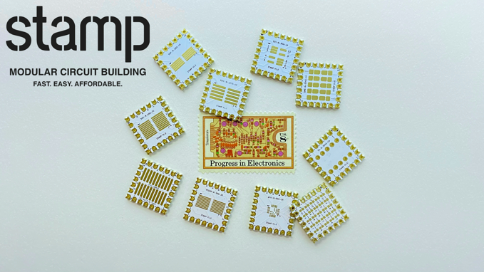
[Kalesh Sasidharan] from Sciotronics wrote in to tell us about their project, Stamp: a modular set of template breakout boards designed to make prototyping with SMD components faster, easier, and more affordable. No breadboards, custom PCBs, or tangled jumper wires required. The project has blasted past its Kickstarter goal, and is on track to start shipping in September.
Stamp was created out of frustration with the traditional SMD prototyping workflow. Breadboards don’t support SMD parts directly, and using adapters quickly gets messy, especially when you need to iterate or modify a design. Ordering PCBs for every small revision just adds delay, and cost.
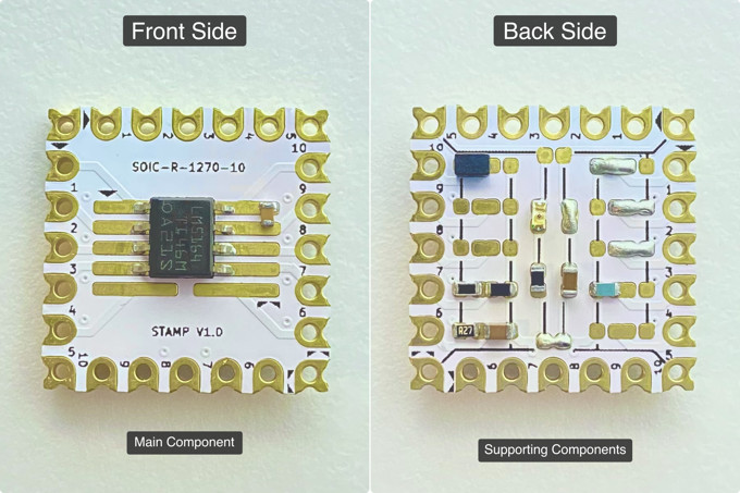 Stamp solves this by offering reusable template boards with commonly used SMD footprints. You place the main component on the front and the supporting components on the back. Many complete circuits, such as buck converters, sensor blocks, microcontrollers, and so on, can fit on a single 17.8 × 17.8 mm board.
Most Stamps feature custom castellated holes, designed for side-by-side or right-angle edge connections, enabling a modular, reconfigurable approach to circuit building. The plan is to make the designs fully open source, so that others can build or adapt them. Although many PCB manufacturers might not have the facilities to make the special castellated edges which are available on some Stamps.
Dave Jones from the EEVblog covered the Stamp on one of his recent Mailbag videos, which you can check out below. This isn’t the first time we’ve seen somebody promise to reinvent the breadboard, but we do appreciate the simplicity of this approach.


Alternative: https://github.com/NNNILabs/Manhattan-Adapters-Prototyping-Ideas
Perhaps not as neat, but cheap.
I usually put the breakouts on an unetched PCB blank, which provides a ground plane. The through-plated pads on this one would make that harder, you’d need some tape in between to insulate.
Also these: https://www.aliexpress.com/item/1005006101886814.html
Yes! We used these kinds of adapters ourselves during prototyping. They actually inspired us to come up with something more streamlined – something that doesn’t rely on a breadboard and lets you add supporting components on the same board. That’s how Stamp came about!
Thanks for sharing that link! Really interesting approach. I see what you mean about using a blank PCB as a ground plane. With Stamp, we tried to sidestep the need for a backing board by making the modules interconnectable – they can be linked edge-to-edge either by direct soldering or with headers/jumper pins.
Looks very much like a solution in search of a problem.
It’s kind of a nice idea. Ive used something sort of similar but for ics with pinouts that wouldn’t ever fit perf board.
fortunately i have lots of problems that need things like this.
I read that as “it’s possible to do that, but not actually a good idea to do that”.
Technically, yeah, it’ll work. But work well?….
Thanks for sharing your thoughts. Stamp actually came out of a real need we kept running into – prototyping with SMD parts often meant dealing with messy jumper wires and fragile adapter setups. We wanted a cleaner, faster and more modular way to prototype – something closer to a breadboard, but made for SMD parts.
seems expensive, anyone got a JLCpcb link?
The doco says they will be releasing the gerber files for the Stamp boards, but to my knowledge they are not available yet. Some manufacturers may not be able to do the fancy castellated edges.
Thanks for raising this! As John mentioned, we will be releasing the Gerber files later this year – Stamp is going fully open-source so the maker community can build on it.
One of the goals of our Kickstarter was to scale production so we could offer Stamp at an accessible price without compromising on quality. We are starting at £1 per Stamp, with ENIG finish and adherence to IPC standards wherever possible to ensure both reliability and consistency.
What do these offer that Schmartboards don’t already do? https://schmartboard.com/
(and pretty darned well)
They have a bunch of clever additions, like pads on the backside with SMT spots that go to VCC/GND, respectively, so you don’t have to add the pullup resistor or decoupling cap off the breakout.
Don’t think I’ll ever buy one of these, but I’ll definitely riff on the theme.
Hmm, the Basic Stamp people (Parallax) might have some concerns about the name.
Yes they are still around :-)
Came here to say that parallax basic stamp was my first MCU 🔥
Thanks so much for pointing that out! We are based in the UK, and the potential name conflict with Parallax’s Basic Stamp hadn’t come up on our radar – especially since our core product is called just Stamp, and “Basic” is only one of the variant names. That said, we really appreciate the heads-up and are actively considering a name change for that variant to avoid any confusion.
I don’t hate the idea, the “stamp” form factor would play well with flexy-pins.
But at over $1 a stamp on kickstarter of all places… this doesn’t make sense to me. IMO, the people most likely to use these are also the same people most likely to be totally comfortable sending off to pcbway/jlcpcb/whatever and getting 100 for the same price.
Would have been more motivated to just give them $20 for the kicad models.
Flexy-pins what?
which sounds like exactly 1 sale before that’s up on a git repo someplace.
Thanks for the thoughtful comment – and fair point about the DIY route. That is actually why we are making Stamp fully open-source later this year, so anyone can build their own or adapt it as needed. We want to support both sides: makers who enjoy building from scratch, and those looking for a faster, more accessible way to prototype.
As for the price, the Kickstarter kit includes 20 boards (2 of each of 10 designs), covering a wide range of popular SMD footprints. Each board features an ENIG finish, custom castellated edges (Regular and Pro), and blind vias (Pro) – not the cheapest to manufacture, but essential for functionality and compactness. We have followed IPC standards wherever possible to ensure reliability.
One of the key goals of the Kickstarter was to scale production and offer Stamp at an accessible price without compromising on quality.
The problem – handling minute components with fat fingers – has been around so long that you can get the solutions (adapter boards) from the usual discount sources that others mention. The only “innovation” seems to be castellated edges to make it into a marketing press-release-friendly form factor. Also likely some trademark/copyright issues with various entities.
All in all this reminds me of student projects that start with self-reassuring cliches and reinvent a commercially available wheel.
Thanks for taking the time to share your thoughts. You are right that SMD adapter boards have been around for a long time, and they work well in many situations. Where Stamp differs is in being a template breakout system designed not just to hold a single component, but to also include supporting circuitry – resistors, capacitors, inductors, etc. – all on the same board. That is what makes rapid prototyping with SMDs much more efficient.
The castellated edges are a key part of that approach – they enable edge-to-edge interconnection, making it easy to build modular prototypes without needing breadboards or jumper wires.
This project came out of years of hands-on frustration with messy SMD prototyping. It was developed by experienced electronics engineers aiming to improve the workflow – not to reinvent the wheel, but maybe to add a few spokes that were missing :)
We really appreciate critical feedback, it helps us explain things better and improve where it counts.
It’s basically HAM Radio Manhattan-style construction.
https://hackaday.com/2011/09/04/a-ham-radio-receiver-manhattan-style/
Fun fact: Radio pirates used “Manhattan Style” construction methods to build their gear decades before it became popular in the ham radio scene. It would often be seen in underground literature to illustrate how to construct transmitters. Part of me wonders if the QRP homebrewers who taught the hams about it may have been those pirates, hihi.
I think it’s more like arts and crafts projects for old men but, hey, it works! :)
Thanks for sharing the link – and the bit of history! Really fascinating to hear how Manhattan-style construction evolved!
Reminds me in a way of Denshi blocks!
https://en.wikipedia.org/wiki/Denshi_block
Ah, now that’s a Proustian moment from my childhood…
Denshi blocks look super interesting! It is great to see how modular circuit building has evolved over time, and how tools like that helped make electronics more accessible for learning and exploration.
I like using the MePADs from https://qrpme.com/, but I generally like to build Manhattan style and these lend themselves to it.
This is an old technique that I love. They used to form towers out of boards this shape.
See https://www.worldradiohistory.com/BOOKSHELF-ARH/Technology/Gernsback/Radiocraft-Technical/GERN-Printed-Circuits-Moses.pdf page 115 fig 382 & 383. Nice to see a modern version.
Thanks for sharing the book — really fascinating! It is amazing to see how electronics has evolved over time and how modular ideas were approached in earlier times. Always inspiring to look back at the roots of the field.
This is a very old technique used to make modular circuits. See page 115 of the following book: https://www.worldradiohistory.com/BOOKSHELF-ARH/Technology/Gernsback/Radiocraft-Technical/GERN-Printed-Circuits-Moses.pdf
Nice to see a modern version!
(Sorry if this is a double post. HaD comments are always booked on my browser.)
Excellent, Thanks ! I had this kind of books when I was a kind, not exactly this one. I just wish for a German version :).
YW. Yes, these type of books inspired my imagination so much as a kid and to be honest they still do. Americanradiohistory.com has a huge library of books and magazines like this and their search is a great way to find obscure adverts, old product/project schematics, etc. it’s inspiring to look at the state of engineering over a century ago.
Now we just need a GermanRadioHistory website for you :)
I think the real benefit people are missing, is not that it breaks out the pins, but that it also offers available strapping options for all of the pins on the board as well. Although it looks like it needs to be 4 layers to accomplish this with this smaller design. I think a design that offered this feature but all the components on the top and also breadboard compatible would be the ideal solution.
Thank you for the thoughtful feedback — you are absolutely right. Stamp uses a 4-layer PCB to achieve the complex routing needed to break out the pins of the main component and provide flexible strapping options to VCC or GND on the back side — either directly or through passive components. Also, the pitch of the Stamp is optimised to be breadboard-compatible, so it can slot into common prototyping workflows as well.