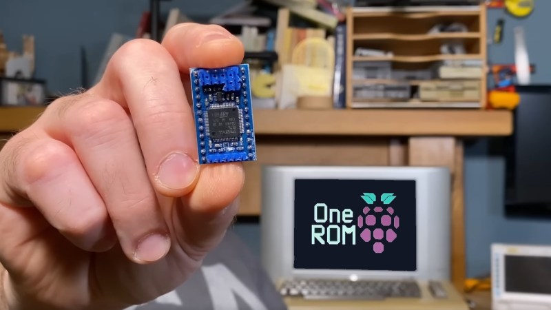
Retrocomputers need ROMs, but they’re just so read only. Enter the latest incarnation of [Piers]’s One ROM to rule them all, now built with a RP2350, because the newest version is 5V capable. This can replace the failing ROMs in your old Commodore gear with this sweet design on a two-layer PCB, using a cheap microcontroller.
[Piers] wanted to use the RP2350 from the beginning but there simply wasn’t space on the board for the 23 level shifters which would have been required. But now that the A4 stepping adds 5 V tolerance [Piers] has been able to reformulate his design.
The C64 in the demo has three different ROMs: the basic ROM, kernel ROM, and character ROM. A single One ROM can emulate all three. The firmware is performance critical, it needs to convert requests on the address pins to results on the data bus just as fast as it can and [Piers] employs a number of tricks to meet these requirements.
The PCB layout for the RP2350 required extensive changes from the larger STM32 in the previous version. Because the RP2350 uses large power and ground pads underneath the IC this area, which was originally used to drop vias to the other side of the board, was no longer available for signal routing. And of course [Piers] is constrained by the size of the board needing to fit in the original form factor used by the C64.
The One ROM code is available over on GitHub, and the accompanying video from [Piers] is an interesting look into the design process and how tradeoffs and compromises and hacks are made in order to meet functional requirements.
Thanks to [Piers] for writing in to let us know about the new version of his project.


Why would you use 2-layer today when 4-layer boards are practically free?
It does give the option of etching or cutting it yourself, which is non-trivial if you are very remote or have a time sensitive repair.
why use 4 layer if you don’t need it?
okay, I’ll bite. I pay $1.04/board shipped for 2-layer boards ($0.72/board before orange man) for small single-board orders.
for 4-layer, it doubles the price (more than triples the price if we exclude shipping). Where is it “practically free”, and what is the shipped price per board?
+1. Also, as I say in the video, I don’t think 4 layer helps here – you still can’t route on the top layer due to the RP2350, the middle layers are ground and power, so you’re still stuck with the bottom layer and the vias going through the chip’s ground pad. So you need to go with 6 layers to make your life easier – but it’s unnecessary as I’ve shown.
I wrote a detailed answer with JLCPCB quotes, etc. The text box turned white with an error message and the text was gone, just as I was about to copy it because of the eccentricities of HaD.
The upshot was that the minimum 5 piece order with shipping, 2 layer was a little less the 4 layer at about $5 each. If there is a shipping option other than DHL, it is much cheaper. A 100 piece order is about 70 cents per 4 layer board and shipping added brings it to less than $1.35. 25x60mm.
Plus there are some assembly options. https://jlcpcb.com/raspberry-pi-rp2350
For cost sensitive versus time tradeoffs there must be someone in Shenzhen who will pick up orders at JLCPCB and send them China Post for a small fee.
Wow! Thanks for taking the time with that. That’s definitely not terrible at all for sizeable orders.
Well, 5V tolerant but not like this. From the RP2350 data sheet:
Fault Tolerant Digital. These pins are described as Fault Tolerant,
which in this case means that very little current flows into the pin
whilst it is below 3.63 V and IOVDD is 0 V. Additionally, they will
tolerate voltages up to 5.5 V, provided IOVDD is powered to 3.3 V.
Since the 3.3V regulator runs off the 5V in this design there is plenty of time for 5V to fry your GPIOs before the IOVDD is up and stable at 3.3V.
Will it work anyway? Maybe, probably, who knows? It’s not to spec anyway.
It depends greatly on the actual logic levels driving pins on the ROM. Most TTL IC datasheets show logic high as 3.4-ish volts or less, depending on the specific family. Pull-ups and hard-wired pins might be an issue, but in practice even the old 2340 put up with a fair amount of abuse.
I wouldn’t build and sell this design by the thousands, but as a hobbyist-level retro-computing tool, it’s pretty awesome.
Agree. .As you say, this isn’t the most robust solution – the other related issue is that the abs max voltage on the RP2350 is 5.5V. Those old ICs, and the STM32 which I already have a solution based on, has an abs max voltage up to >7V. So, one dodgy voltage regulator and …
On the other hand, I haven’t fried an RP2350 yet, and I’ve done quite a lot of testing, including for example as the C64 char ROM, which has one of the CS lines permanently pulled to 5V. Maybe I’m damaging the GPIO pads a brief instant at a time, and it’ll catch up with me.
It’s highly likely that other manufacturer’s microcontrollers with 5v-tolerant inputs have exactly the same restrictions, but the manufacturer doesn’t bother to mention it. And yet they’re still routinely used in such applications without problems. The “fault tolerant” mechanism relies on IOVDD to prevent current flow into the pin at 5V, but it’s not the only mechanism present. These pins all have ESD protection diodes present for transient voltage spikes far above 5V, and they’ll also protect the pin – they just do it by conducting to the rail, so the “low current flow into the pin” feature is not present, but the pin is still protected.
Unless you have actual evidence that there’s any real risk of damage in normal use, you’re just making up reasons to rag on a product you don’t like.
As it is, even the RP2040 has similar behaviour, just not “officially” (because Raspberry Pi did not spend the money to validate it), and I’ve used them in 5v systems with zero issues.
Is anyone going to mention that this is a big change in the Absolute Maximum Ratings for some pins and they’re just calling it a “stepping?” Seriously, change it to “RP2350A” or “RP2355” or something.
There is no change except fixing the E9 bug. They confirmed the same 5v tolerance applies to previous steppings, there is no HW change done for 5v tolerance, they just bothered to validate it.
Nice work. I especially appreciate the work on /reading/ the data sheet to find exploitable behaviors. FWIW, it might be fine to put bypass caps on the backside of the board as the legs of the ROM may be made long enough to reach.
You’d definitely be able to put components on the underside – but top and bottom assembly is more expensive than just top.
Amazing a dual core (quad core?) multiple hundred Mhz SoC and its PCB are cheaper than a PROM now!
Any chance you can add peripherals or virtual drives on the ROM socket of these systems?
While you can do stuff like change the ROM images on the fly, the ROM sockets don’t give you great flexibility for extending the retro system. You really want to be jacked into the cartridge port, IEC port, etc, to give you the greatest flexibility. If you’re into C64s and haven’t already, check out Meatloaf.
No inherently 5V MCU has enough on-chip memory, IO lines, and speed to do the job?
c64 had kernal, not kernel like linux
What is the difference? I’ve never heard ‘kernal’ before now :)
Originally “KERNAL” was just a typo in the manual for the Commodore PET 2001, this wasn’t noticed and copied to other machines. Later when the typo was discovered they decided to stick with it and created the backronym „Keyboard Entry Read, Network, And Link“.
With the Amiga they changed back to “Amiga ROM Kernel”, but often it was called Kickstart, Kickrom or just Kick .
Probably naive, but could you put diodes to ground on each pin so they cap at lower voltage?
All this stuff is fine, but where are the timings diagrams showing this thing responds and returns data at the necessary timings to replace the ROM.
I’m very infused how the character ROM is using the same data lines as the CPU. I assume it isn’t really a character ROM, more a character set look up table which is read by the CPU to work on a pixel display.
I think author cares mainly about Commodore 8bitters and RP2350 being fast enough for C64 was the goal here. There is also $3 ESP32-C3 based Airfrog companion project to go with OneRom allowing you to one click reprogram over the air. Pretty slick.
Project looks fantastic. Optimized to the bone, coded to bare metal, cheap, easy to replicate, open source.
I also made a ROM emulator using RP2350 (Pico2), check it out!
https://hackaday.io/project/203946-pico2romemu-rp2350pico2-rom-emulator