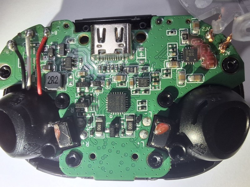
Wireless earbuds are notoriously tiny. Want to see inside? [MCH170] did and published a Soundcore Space A40 Teardown.
In this teardown, you’ll see inside the charging case and one of the earbuds. Starting with the case, removing the back cover revealed the charging coil and a few screws holding the PCB in place. Removing the screws allows for removing the coil. The main PCB and the magnets that hold the earbuds in place are then visible. The microcontroller is an SS881Q from Sinhmicro. The back side of the main circuit board has a handful of SMD components, including some status LEDs. The battery is a 13450 with a nominal voltage of 3.72V and a capacity of 800mAh or 2.967Wh.
He then goes on to have a look inside one of the earbuds, which were not working prior to disassembly. The earbuds are held together with friction clips. The top of the PCB has two ribbon cables that need to come off. The top ribbon connects to the battery, and the bottom one is for the speaker and charging connections. The three pogo pins connect the touch sensor, which is installed in the outer casing. The back of the PCB is densely populated with SMD components. The main IC is a WQ7033AX Bluetooth audio SoC from WUQI Microelectronics. Under the PCB, we find the battery and the speaker. The battery has a nominal voltage of 3.85V and a capacity of 53mAh, equivalent to 0.204Wh.
All in all, an interesting look into some fairly state-of-the-art technology! If you’re interested in earphones, you might like to check out Cheap DIY High Impedance Earphones. Or, perhaps you’d rather convert an old pair to twice as much wireless.


huh. i think i’m about as negative on videos as anyone possibly could be. and i’m certainly critical of empty content.
but i was curious as i read the hackaday article and i got more information of interest to me out of the article than out of your summary. and then, i clicked through to the teardown. and would you believe, it isn’t a video at all? it’s a simple website with a bit of text and a series of high resolution photographs. which is just about the height of what i hope for from a little write up like this one so
i’m always curious about the frontier of miniaturization and i’m certainly tickled to see that even something as tiny as an in-ear device still can “waste a ton of space” on connectors. given how small they are i wouldn’t’ve been surprised to see the chip soldered directly onto the battery somehow so it’s fun to see how they actually did it
Nice photos and actual article. Teardowns are always welcome: )
Yes, I also love a good teardown!