Castellated PCB edges are kind of magical. The plated semicircular features are a way to make a solid, low-profile connection from one board to another, and the way solder flows into them is deeply satisfying. But adding them to a PCB design isn’t always cheap. No worries there — you can make your own castellations with this quick and easy hack.
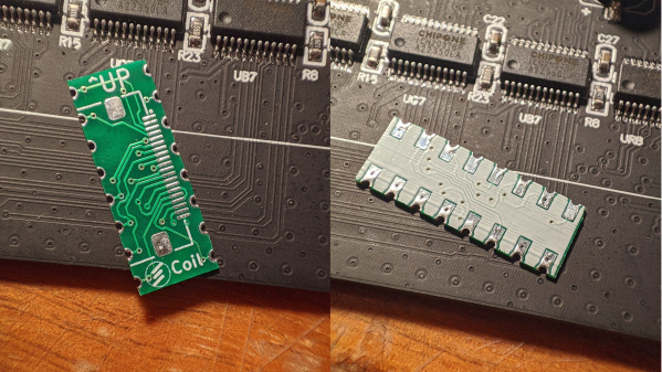
 [@CoilProtogen] doesn’t include much information in the Twitter thread about design details, but the pictures make it clear what the idea is here. OEM castellations are really just plated areas at the edge of a board that can be used to tack the board down to another one without any added hardware. The hack here is realizing that lining up a bunch of large-diameter vias and cleaving them in half with a sharp pair of scissors will result in the same profile without the added cost. The comments on the thread range from extolling the brilliance of this idea to cringing over the potential damage to the board, but [@CoilProtogen] insists that the 0.6-mm substrate cuts like butter. We’d worry that the plating on the vias would perhaps tear, but that seems not to be the case here.
The benefits of a zero-profile connection are pretty clear in this case, where castellated PCBs were used to replace bulky header-pin connectors on a larger PCB. We can see this technique being generally useful; we’ve seen them used to good effect before, and this is a technique we’ll keep in mind for later.