More Details On That First Home-Made Lithographically Produced IC

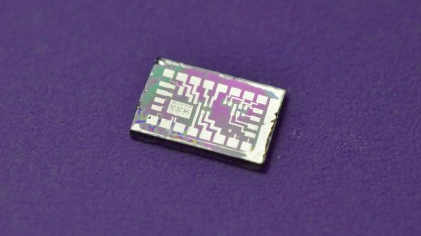
A few days ago we brought you news of [Sam Zeloof]’s amazing achievement, of creating the first home-made lithographically produced integrated circuit. It was a modest enough design in a simple pair of differential amplifiers and all we had to go on was a Twitter announcement, but it promised a more complete write-up to follow. We’re pleased to note that the write-up has arrived, and we can have a look at some of the details of just how he managed to produce an IC in his garage. He’s even given it a part number, the Zeloof Z1.

For ease of manufacture he’s opted for a PMOS process, and he is using four masks which he lists as the active/doped area, gate oxide, contact window, and top metal. He takes us through 66 different processes that he performs over the twelve hours of a full production run, with comprehensive descriptions that make for a fascinating run-down of semiconductor manufacture for those of us who will never build a chip of our own but are still interested to learn how it is done. The chip’s oblong dimensions are dictated by the constraints of an off-the-shelf Kyocera ceramic chip carrier, though without a wire bonding machine he’s unable to do any more than test it with probes.

You can read our reporting of his first announcement, but don’t go away thinking that will be all. We’re certain [Sam] will be back with more devices, and can’t wait to see the Z2.

First Lithographically Produced Home Made IC Announced

It is now six decades since the first prototypes of practical integrated circuits were produced. We are used to other technological inventions from the 1950s having passed down the food chain to the point at which they no longer require the budget of a huge company or a national government to achieve, but somehow producing an integrated circuit has remained out of reach. It’s the preserve of the Big Boys, move on, there’s nothing to see here.

Happily for us there exists a dedicated band of experimenters keen to break that six-decade dearth of home-made ICs. And now one of them, [Sam Zeloof], has made an announcement on Twitter that he has succeeded in making a dual differential amplifier IC using a fully lithographic process in his lab. We’ve seen [Jeri Ellsworth] create transistors and integrated circuits a few years ago and he is at pains to credit her work, but her interconnects were not created lithographically, instead being created with conductive epoxy.

For now, all we have is a Twitter announcement, a promise of a write-up to come, and full details of the lead-up to this momentous event on [Sam]’s blog. He describes both UV lithography using a converted DLP projector and electron beam lithography using his electron microscope, as well as sputtering to deposit aluminium for on-chip interconnects. We’ve had an eye on his work for a while, though his progress has been impressively quick given that he only started amassing everything in 2016. We look forward to greater things from this particular garage.