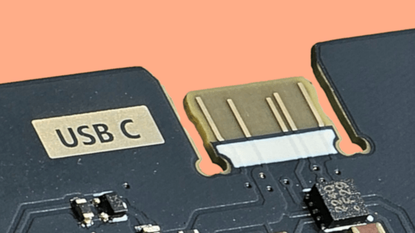
Sometimes when you’re making a PCB that you plan on programming over USB, but you only plan on plugging in a couple of times, it would be nice to make that connection without another BOM item. Over on GitHub [AnasMalas] has released a PCB edge USB-C connection symbol/footprint to do just that!
This isn’t the first PCB edge USB-C connector we’ve seen, but this one has some nice features. It’s available in both KiCad and EasyEDA formats, allowing you to easily add it into your preferred ECAD software. As well as supporting multiple software packages, there are two versions included: a 10-pin and 14-pin version. The 10-pin version has, on each side, 2 USB voltage pins, 2 ground pins, and a CC1 or CC2 pin on its respective side; this version is ideal if you’re looking to just supply power via the connector. The 14-pin version has all the pins of the 10-pin version with the addition of four data-positive and data-negative pins needed to relay information to the board, ideal if you’re planning on programming a microcontroller with this connection.
One important note is that, while most PCBs default to 1.6 mm thickness, if you use this connector you’ll need to drop that down to ~0.8 mm to properly interface with a common USB cable. [AnasMalas] also suggests using ENIG board finish to preserve the connectors on your USB cable.
For such a small and common connector, USB-C holds a ton of potential. Be sure to check out our series all about USB-C for more details.
Thanks to [Ben] for the tip.