To err is human. And to order the wrong component foot print is just part of engineering. It happens to us all; You’re working hard to finish a design, you have PCBs on the way and you’re putting in your order into your favorite parts supplier. It’s late, and you’re tired. You hit submit, and breathe a sigh of relief. Little do you know that in about a week when everything arrives, that you’ll have ordered the wrong component package for your design.
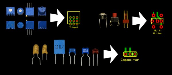
Well, fear not. [David Cook] has a solution that could save your bacon. He shows you how to design multiple footprints into your board to avoid the most common mistakes such as voltage regulators with different pin-outs than expected. Other uses for the trick include, common trim pots with different pin spacing and a layout for decoupling caps that will fit both a 0.1″ and 0.2″ footprints.
We’ll file this under the “Why Didn’t I Think of That” category. It’s a super simple hack, but that’s what we love about it. We could see this being very handy for people who often scavenge parts. Also, for makers that sell just a bare PCBs (without parts) to those that want just a board. No, it won’t save you if your need an SMD and you mistakenly ordered a dip, but at the end of the day, it’s a nice trick to keep up your sleeve. You might never know when you’ll need it.


