Designing your own integrated circuits as a one-person operation from your home workshop sounds like science fiction. But 20 years ago, so did rolling your own circuit boards to host a 600 MHz microcontroller with firmware you wrote yourself. Turns out silicon design isn’t nearly as out of reach as it used to be and Matt Venn shows us the ropes in his Zero to ASIC workshop.
Held during the 2020 Hackaday Remoticon, this is a guided tour of the tools used in the Skywater PDK — the Process Design Kit that is an open-source ASIC toolkit produced in a partnership between Google and SkyWater Technology. We covered the news when first announced back in June, but this the most comprehensive look we’ve seen into the actual design process.
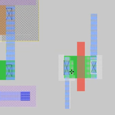
Matt builds up the demo starting from the very simple design of an N-channel MOSFET with click-and-drag tools similar to graphics editing software. The good news it that although you can draw your own structures like this, for digital designs you won’t have to. A wide variety of IP has been contributed to the open source project allowing basic building blocks to be pulled in using HDL. However, the power of drawing structures will certainly be the playground for those needing analog design as part of their projects.
As with EDA software used for circuit boards, the PDK includes design rule checks to ensure you aren’t violating the limits of the 130 nm chip fab. There’s some other black magic in there too, as Matt specifically mentions an antenna rules check to safeguard your design from being fried by induced current on “large” (microscopically so) metalized runs during the fabrication process.

The current workflow involves grinding through a large number of configuration files, something Matt admits took him a long time to wrap his head around. However, what’s available for proofing your design is very impressing. He demonstrates SPICE simulation to calculate timings, and shows numerous examples of verification drawings generated by the compilation process, either in the form of seeing the structures as they will be laid out, or as logical flow charts. This is crucial as a single run will take 2-3 months to come back from fab — you want to get things right before buttoning up the project. Incidentally, that’s know as “tapeout”, a term you’ve likely heard before and he says it comes from reels of magnetic tape containing the design being removed from the computer and sent to production. Who knew? (This tidbit in strikethrough appears to be incorrect).
But wait, there’s more to this than just designing the things. Part of the intrigue of the Skywater-PDK project is that Google bought into covering a group run about once per quarter so that open-source designs can be ganged onto a multi-project wafer free of charge to the people submitting them. That’s pretty awesome and we’re giddy to hear news of people getting their wafer-level chip scale devices — also known as flip chips — back for testing. Matt is planning a more in-depth paid course on the topic. For now, get a taste of what’s involved from this excellent workshop found after the break.
Continue reading “Remoticon Video: From Zero To ASIC; How To Design In Silicon”


