More 3D Printed IKEA Hacks Make Life Better

There’s an old joke that the CEO of IKEA is running to be Prime Minister of Sweden. He says he’ll be able to put together his cabinet in no time. We don’t speak Swedish, but [Adam Miklosi] tells us that the word “uppgradera” means “upgrade” in Swedish. His website, uppgradera.co has several IKEA upgrade designs you can 3D print.

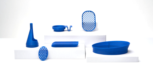
There are currently six designs that all appear to be simple prints that have some real value. These are all meant to attach to some IKEA product and solve some consumer problem.

For example, the KL01 is a cup holder with a clip that snaps into the groove of a KLIPSK bed tray. Without it, apparently, your coffee mug will tend to slide around the surface of the tray. The CH01 adds a ring around a cheese grater. There are drains for a soap dish and a toothbrush holder, shoulder pads for coat hangers, and a lampshade.

We worry a little about the safety of the cheese grater and the toothbrush because you will presumably put the cheese and the toothbrush into your mouth. Food safe 3D printing is not trivial. However, the other ones look handy enough, and we know a lot of people feel that PLA is safe enough for things that don’t make a lot of contact with food.

Honestly, none of these are going to change your life, but they are great examples of how simple things you can 3D print can make products better. People new to 3D printing often seem to have unrealistic expectations about what they can print and are disappointed that they can’t easily print a complete robot or whatever. However, these examples show that even simple designs that are easily printed can be quite useful.

If you don’t have a printer, it looks like as though site will also sell you the pieces and they aren’t terribly expensive. We don’t know why IKEA invites so many hacks, but even they provide 3D printer files to improve the accessibility of some products.

High Tech Photos Capture Snowflakes Like Never Before

Microscopy used to be a rarity in the hobby electronics world. But anyone doing lab work has always needed a microscope and with today’s tiny parts, it is almost a necessity. However, [Nathan Myhrvold] didn’t use an ordinary microscope to capture some beautiful snowflake pictures. According to [My Modern Met], the pictures are the highest resolution snowflake pictures ever taken.

Of course, the site is more interested in the visual aspect of it, but they did provide some clues about the tech behind the pictures. According to the site:

Myhrvold used a special camera of his own design. He combined the magnifying power of a microscopic lens.. with a specially designed optical path. This path allowed the lens to channel its image to a medium-format digital sensor… In addition, the camera featured a cooling stage upon which the tiny specimens could rest. With LED short-pulse lights and a shutter speed of less than 500 microseconds, Myhrvold was able to capture multiple images of each snowflake at different focal lengths. These images were then stacked to create the final image.

Continue reading “High Tech Photos Capture Snowflakes Like Never Before”

Federal Aviation Administration Announces Major Drone Rule Changes

If new rules from the FAA regarding unmanned aircraft operations in the US are any indication, drones are becoming less of a niche hobby and more integrated into everyday life. Of course, the devil is in the details, and what the Federal Aviation Administration appears to give with one hand, it takes away with the other.

The rule changes, announced on December 28, are billed as “advanc[ing] safety and innovation” of the drone industry in the United States. The exciting part, and the aspect that garnered the most attention with headline writers, is the relaxation of rules against night operation and operating above people and moving vehicles. Since 2016, it has been against FAA regulations to operate drones less than 55 pounds (25 kg) at night or over people without a waiver. This rule can be seen as stifling innovations in drone delivery, since any useful delivery service will likely need to overfly populated areas and roadways and probably do so at night. The new rules allow these operations without a waiver for four categories of drones, classified by how much damage they would do if they were to lose control and hit someone. The rules also define the inspection and certification regimes for both aircraft and pilot, as well as stipulating that operators have to have their certificate and ID on their person while flying.

While this seems like great news, the flip side of the coin is perhaps less shiny. The rule changes also impose the requirement for “Remote ID” (PDF link), which is said to be “a major step toward full integration of drones into the national airspace system.” Certain drones will be required to carry a system that transmits identification messages directly from the aircraft, including such data as serial number, location and speed of the drone, as well as the location of the operator. The rules speculate that this would likely be done over WiFi or Bluetooth, and would need to be receivable with personal wireless devices. The exact technical implementation of these rules is left as an exercise to manufacturers, who have 30 months from the time the rules go into effect in January to design systems, submit them for certification, and get them built into their aircraft. Drone operators have an additional year to actually start using the Remote ID drones.

For the drone community, these rule changes seem like a mixed bag. To be fair, it’s not exactly unexpected that drones would be radio tagged like this, and the lead time allowed by the FAA for compliance on Remote ID seems generous. The ability to operate in riskier environments will no doubt be welcomed by commercial drone operators. So who knows — maybe the rules will do what they say they will, and this will stimulate a little innovation in the industry. If so, it could make this whole thing a net positive.

Magnetic Motorized Plasma Cutter Track

Affordable plasma cutters are becoming a popular step up from an angle grinder for cutting sheet metal in the home workshop, but cutting long straight lines can be laborious and less than accurate. [Workshop From Scratch] was faced with this problem, so he built a motorized magnetic track for his plasma cutter.

Thanks to a pair of repurposed electromagnetic door looks and adjustable base width, the track can be mounted on any piece of magnetic steel. The track itself consists of a pair of linear rods, with the torch mounts sliding along on linear bearings. A lead screw sits between the two linear rods, and is powered by an old cordless drill with the handle cut off. Its trigger switch was replaced by a speed controller and two-way switch for direction control, and a power supply took the place of the battery. The mounting bracket for the plasma torch is adjustable, allowing the edge of the steel to be cut at an angle if required.

While limit switches on the end of the track might be a preferable option to prevent sliding base to hit the ends of the tracks, the clutch in the electric drill should be good enough to prevent damage if the operator is distracted.

[Workshop From Scratch] is really living up to the name of his YouTube channel, having built many of the other tools used in the video himself. Just a few examples are the XY-table, hydraulic adjustable workbench and  hydraulic shop crane. Continue reading “Magnetic Motorized Plasma Cutter Track”

Remoticon Video: From Zero To ASIC; How To Design In Silicon

Designing your own integrated circuits as a one-person operation from your home workshop sounds like science fiction. But 20 years ago, so did rolling your own circuit boards to host a 600 MHz microcontroller with firmware you wrote yourself. Turns out silicon design isn’t nearly as out of reach as it used to be and Matt Venn shows us the ropes in his Zero to ASIC workshop.

Held during the 2020 Hackaday Remoticon, this is a guided tour of the tools used in the Skywater PDK — the Process Design Kit that is an open-source ASIC toolkit produced in a partnership between Google and SkyWater Technology. We covered the news when first announced back in June, but this the most comprehensive look we’ve seen into the actual design process.

Drawing N-channel MOSFET in silicon

Matt builds up the demo starting from the very simple design of an N-channel MOSFET with click-and-drag tools similar to graphics editing software. The good news it that although you can draw your own structures like this, for digital designs you won’t have to. A wide variety of IP has been contributed to the open source project allowing basic building blocks to be pulled in using HDL. However, the power of drawing structures will certainly be the playground for those needing analog design as part of their projects.

As with EDA software used for circuit boards, the PDK includes design rule checks to ensure you aren’t violating the limits of the 130 nm chip fab. There’s some other black magic in there too, as Matt specifically mentions an antenna rules check to safeguard your design from being fried by induced current on “large” (microscopically so) metalized runs during the fabrication process.

Part of a massive logic flow chart for an IC counter design

The current workflow involves grinding through a large number of configuration files, something Matt admits took him a long time to wrap his head around. However, what’s available for proofing your design is very impressing. He demonstrates SPICE simulation to calculate timings, and shows numerous examples of verification drawings generated by the compilation process, either in the form of seeing the structures as they will be laid out, or as logical flow charts. This is crucial as a single run will take 2-3 months to come back from fab — you want to get things right before buttoning up the project. Incidentally, that’s know as “tapeout”, a term you’ve likely heard before and he says it comes from reels of magnetic tape containing the design being removed from the computer and sent to production. Who knew? (This tidbit in strikethrough appears to be incorrect).

But wait, there’s more to this than just designing the things. Part of the intrigue of the Skywater-PDK project is that Google bought into covering a group run about once per quarter so that open-source designs can be ganged onto a multi-project wafer free of charge to the people submitting them. That’s pretty awesome and we’re giddy to hear news of people getting their wafer-level chip scale devices — also known as flip chips — back for testing. Matt is planning a more in-depth paid course on the topic. For now, get a taste of what’s involved from this excellent workshop found after the break.

Continue reading “Remoticon Video: From Zero To ASIC; How To Design In Silicon”

Seeking Enlightenment: The Quest To Restore Vision In Humans

Visual impairment has been a major issue for humankind for its entire history, but has become more pressing with society’s evolution into a world which revolves around visual acuity. Whether it’s about navigating a busy city or interacting with the countless screens that fill modern life, coping with reduced or no vision is a challenge. For countless individuals, the use of braille and accessibility technology such as screen readers is essential to interact with the world around them.

For refractive visual impairment we currently have a range of solutions, from glasses and contact lenses to more permanent options like LASIK and similar which seek to fix the refractive problem by burning away part of the cornea. When the eye’s lens itself has been damaged (e.g. with cataracts), it can be replaced with an artificial lens.

But what if the retina or optic nerve has been damaged in some way? For individuals with such (nerve) damage there has for decades been the tempting and seemingly futuristic concept to restore vision, whether through biological or technological means. Quite recently, there have been a number of studies which explore both approaches, with promising results.

Continue reading “Seeking Enlightenment: The Quest To Restore Vision In Humans”

Reverse Engineering Silicon From The First Pocket Calculator

We’ve seen so many explorations of older semiconductors at the hands of [Ken Shirriff], that we know enough to expect a good read when he releases a new one. His latest doesn’t disappoint, as he delves into the workings of one of the first hand-held electronic calculators. The Sharp EL-8 from 1969 had five MOS ICs at its heart, and among them the NRD2256 keyboard/display chip is getting the [Shirriff] treatment with a decapping and thorough reverse engineering.

The basic functions of the chip are explained more easily than might be expected since this is a relatively simple device by later standards. The fascinating part of the dissection comes in the explanation of the technology, first in introducing the reader to PMOS FETs which required a relatively high negative voltage to operate, and then in explaining its use of four-phase logic. We’re used to static logic that holds a state depending upon its inputs, but the technologies of the day all called for an output transistor that would pull unacceptable current for a calculator. Four phase logic solved this by creating dynamic gates using a four-phase clock signal, relying on the an output capacitor in the gate to hold the value. It’s a technology that lose out in the 1970s as later TTL and CMOS variants arrived that did not have the output current drain. Fascinating stuff!

[Ken] gave a talk at the Hackaday Superconference a couple of years ago, if you’ve not seen it then it’s worth a watch.