If you have three hours and you want to learn the fundamentals of semiconductors, [Tiny Tapeout] has something for you: An introduction to SiliWiz. You’ll also need the SiliWiz software (or use it online), which resembles the kind of tools that chip designers use but is meant for students to use as a learning tool
Using SiliWiz, you create layers on a virtual device, and you can use Spice to view the results. The tutorial is meant to be high-level and is suggested for students aged 14 or over (but we liked it and we are quite a bit older than that). Some more advanced material is also available at the same site.
Designing your own integrated circuits as a one-person operation from your home workshop sounds like science fiction. But 20 years ago, so did rolling your own circuit boards to host a 600 MHz microcontroller with firmware you wrote yourself. Turns out silicon design isn’t nearly as out of reach as it used to be and Matt Venn shows us the ropes in his Zero to ASIC workshop.
Held during the 2020 Hackaday Remoticon, this is a guided tour of the tools used in the Skywater PDK — the Process Design Kit that is an open-source ASIC toolkit produced in a partnership between Google and SkyWater Technology. We covered the news when first announced back in June, but this the most comprehensive look we’ve seen into the actual design process.
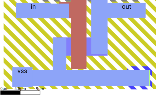
Drawing N-channel MOSFET in silicon
Matt builds up the demo starting from the very simple design of an N-channel MOSFET with click-and-drag tools similar to graphics editing software. The good news it that although you can draw your own structures like this, for digital designs you won’t have to. A wide variety of IP has been contributed to the open source project allowing basic building blocks to be pulled in using HDL. However, the power of drawing structures will certainly be the playground for those needing analog design as part of their projects.
As with EDA software used for circuit boards, the PDK includes design rule checks to ensure you aren’t violating the limits of the 130 nm chip fab. There’s some other black magic in there too, as Matt specifically mentions an antenna rules check to safeguard your design from being fried by induced current on “large” (microscopically so) metalized runs during the fabrication process.
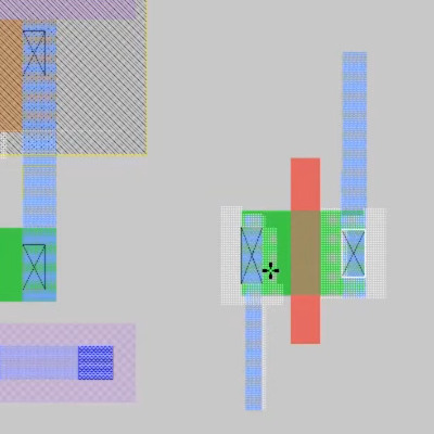
Part of a massive logic flow chart for an IC counter design
The current workflow involves grinding through a large number of configuration files, something Matt admits took him a long time to wrap his head around. However, what’s available for proofing your design is very impressing. He demonstrates SPICE simulation to calculate timings, and shows numerous examples of verification drawings generated by the compilation process, either in the form of seeing the structures as they will be laid out, or as logical flow charts. This is crucial as a single run will take 2-3 months to come back from fab — you want to get things right before buttoning up the project. Incidentally, that’s know as “tapeout”, a term you’ve likely heard before and he says it comes from reels of magnetic tape containing the design being removed from the computer and sent to production. Who knew? (This tidbit in strikethrough appears to be incorrect).
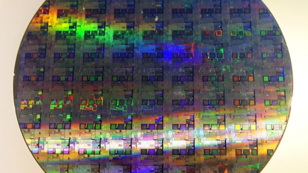
But wait, there’s more to this than just designing the things. Part of the intrigue of the Skywater-PDK project is that Google bought into covering a group run about once per quarter so that open-source designs can be ganged onto a multi-project wafer free of charge to the people submitting them. That’s pretty awesome and we’re giddy to hear news of people getting their wafer-level chip scale devices — also known as flip chips — back for testing. Matt is planning a more in-depth paid course on the topic. For now, get a taste of what’s involved from this excellent workshop found after the break.
You might have caught Maya Posch’s article about the first open-source ASIC tools from Google and SkyWater Technology. It envisions increased access to make custom chips — Application Specific Integrated Circuits — designed using open-source tools, and made real through existing chip fabrication facilities. My first thought? How much does it cost to tape out? That is, how do I take the design on my screen and get actual parts in my hands? I asked Google’s Tim Ansel to explain some more about the project’s goals and how I was going to get my parts.
The goals are pretty straightforward. Tim and his collaborators would like to see hardware open up in the same way software has. The model where teams of people build on each other’s work either in direct collaboration or indirectly has led to many very powerful pieces of software. Tim’s had some success getting people interested in FPGA development and helped produce open tools for doing so. Custom ASICs are the next logical step.
A process design kit (PDK) is a by now fairly standard part of any transformation of a new chip design into silicon. A PDK describes how a design maps to a foundry’s tools, which itself are described by a DRM, or design rule manual. The FOSSi foundation now reports on a new, open PDK project launched by Google and SkyWater Technology. Although the OpenPDK project has been around for a while, it is a closed and highly proprietary system, aimed at manufacturers and foundries.
The SkyWater Open Source PDK on Github is listed as a collaboration between Google and SkyWater Technology Foundry to provide a fully open source PDK and related sources. This so that one can create manufacturable designs at the SkyWater foundry, that target the 130 nm node. Open tools here should mean a far lower cost of entry than is usually the case.
Although a quite old process node at this point (~19 years), it should nevertheless still be quite useful for a range of applications, especially those that merge digital and analog circuitry. SkyWater lists their SKY130 node technology stack as:
Support for internal 1.8V with 5.0V I/Os (operable at 2.5V)
1 level of local interconnect
5 levels of metal
Inductor-capable
High sheet rho poly resistor
Optional MiM capacitors
Includes SONOS shrunken cell
Supports 10V regulated supply
HV extended-drain NMOS and PMOS
It should be noted that use of this open source PDK is deemed experimental at this point in time, and should not be used for any commercial or otherwise sensitive applications.