We’re used to reflow soldering of our PCBs at the hacker level, for quite a few years people have been reflowing with toaster ovens, skillets, and similar pieces of domestic equipment and equipping them with temperature controllers and timers. We take one or two boards, screen print a layer of solder paste on the pads by using a stencil, and place our surface-mount components with a pair of tweezers before putting them in the oven. It’s a process that requires care and attention, but it’s fairly straightforward once mastered and we can create small runs of high quality boards.
But what about the same process at a professional level, what do you do when your board isn’t a matchbox-sized panel from OSH Park with less than 50 or so parts but a densely-packed multilayer board about the size of a small tablet computer and with many hundreds of parts? In theory the same process of screen print and pick and place applies, but in practice to achieve a succesful result a lot more care and planning has to go into the process.
This is being written the morning after a marathon session encompassing all of the working day and half of the night. I was hand-stuffing a row of large high-density boards with components ranging from 0402 passives to large QFPs and everything else in between. I can’t describe the board in question because it is a commercially sensitive prototype for the industrial customer of the friend I was putting in the day’s work for, but it’s worth going through the minutiae of successfully assembling a small batch of prototypes at this level. Apologies then, any pictures will be rather generic.


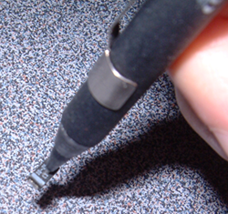
 [K.C. Lee] is busy working on his entry to The Hackaday Prize, and right now he’s dealing with a lot of assembly. For his entry, that means tiny SMD parts, and the vacuum pen he ordered from DealExtreme hasn’t come in yet. The solution?


