[Andrew] has been busy running a class on hardware reverse engineering this semester, and figured a great end for the class would be something extraordinarily challenging and amazingly powerful. To that end, he’s editing CPLDs in circuit, drilling down to metal layers of a CPLD and probing the signals inside. It’s the ground work for reverse engineering just about every piece of silicon ever made, and a great look into what major research labs and three-letter agencies can actually do.
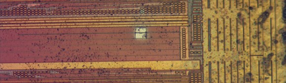
The chip [Andrew] chose was a Xilinx XC2C32A, a cheap but still modern CPLD. The first step to probing the signals was decapsulating the chip from its plastic prison and finding some interesting signals on the die. After working out a reasonable functional diagram for the chip, he decided to burrow into one of the lines on the ZIA, the bus between the macrocells, GPIO pins, and function blocks.
Actually probing one of these signals first involved milling through 900 nm of silicon nitride to get to a metal layer and one of the signal lines. This hole was then filled with platinum and a large 20 μm square was laid down for a probe needle. It took a few tries, but [Andrew] was able to write a simple ‘blink a LED’ code for the chip and view the s square wave from this test point. not much, but that’s the first step to reverse engineering the crypto on a custom ASIC, reading some undocumented configuration bits, and basically doing anything you want with silicon.
This isn’t the sort of thing anyone could ever do in their home lab. It’s much more than just having an electron microscope on hand; [Andrew] easily used a few million dollars worth of tools to probe the insides of this chip. Still, it’s a very cool look into what the big boys can do with the right equipment.


FIBs are the blue wire of the chip industry. When I worked for $BIG_CPU_VENDOR it was not uncommon to have a handful of FIB’d parts made up to workaround design issues to validate a fix and keep development rolling along until the next spin.
You guys had it easy, though – you knew what the chip did, and had full schematics and layout, coming in. I had to go in blind and figure out which signals did what first ;)
Sir, thank you for making the internet not suck on April Fools Day. I am in your debt.
In all seriousness, that was one of the most interesting write-ups I have read in quite some time. That gives me quite a bit of insight on why FIPS 140-2 level 4 stuff is actually hard to make.
Pretty sure I work at $BIG_CPU_VENDOR. Heard today at a meeting in response to the spec for a value range: “the spec is whatever makes it work.”
I thought value range parts weren’t specced but floor sweepings. They throw thousands of efuse chain bits in every chip so they can turn even the shittiest bin into a value SKU.
To clarify, the question was along the lines of what range of values should we expect to have to apply to a tuning parameter. Block owner’s response was to use whatever made it work. Note I’m trying to avoid identifying the block and not use common in-house names for things :P
Definitely lots of fuse bits, but many were just there for normal binning. The abnormal part was starting a project with 3 SKUs, and ending with a dozen to try to eek a few extra dollars out of the parts that just barely missed a frequency bin.
There’s still the occasional fib-edited part to validate ahead of a new spin, but it’s been much rarer than when I was new. Deprocessing to check for physical failures still happens often enough though.
What is the first rule of fight club?
Just because everyone knows certain evils exist, it doesn’t mean everone should openly talk of said evils.
This kind of stuff makes you a target…
Yeah, except it doesn’t, seeing as Flylogic Engineering (now IOActive) basically founded their company doing exactly this sort of thing. Take off your tinfoil hat, loser.
Maybe not, but when the editor starts throwing in comments about three letter agencies, its not a stretch to imagine who they are talking about. And yes, CPLDs are benign. But when you start running your mouth about combinations of three letter agencies and this type of work, it will get the attention of people you don’t want the attention of, if your are at all smart. But you know, running your mouth about things you shouldn’t makes you cool in some circles. But a complete idiot in the ones that can bite you…
The first step to submission and the death of democracy is to stop talking about things openly because “it might attrack the attention of power players”.
Fuck this – this is science, period. The fact that it might attract the attention of three letters agency is something to talk about for the way they throw away money for useless purposes such as this, not something to fear. If you live in a country where you have reason to fear such a thing, then LEAVE (or try to change things, putting yourself in danger).
^ THIS
That’s all noble and nice, but I for one have seen things that were removed from existence because of getting attention when the crowd started to talk too much about it.
So you can have your stance and nothing else, or can be smart and let the 3-letter ones play in their own yard.
None of this work is really doing anything groundbreaking or amazing, though. Nedospasov and Tarnovsky did some much more sophisticated work at ACM CCS this summer, for example (http://nedos.net/ccs2013.pdf). I’m not defeating any unusual tamper protections, developing any amazing attacks, etc.
You act like military agencies are terrified of chip deprocessing and FIB edits like it’s something they haven’t seen before. There’s a reason DARPA has been smitten with FPGAs for at least the past decade — no physical evidence of the design configuration exists, and the stored config can be cryptographically secured.
If this were a concern, there would be stringent restrictions on foreign nationals working in physical failure analysis labs, but this is not the case. Adjust your tin foil hat, it seems to be cooking your brain in the sun.
Ah, they already know that we know. We know that they know that we know, and they know it. This is commercial stuff. Bloody expensive, and tied up in patents and IP and what-not, but it’s still commercial stuff. You can order an ion-beam from a catalogue if you have the money. This isn’t the sort of stuff people get shot in the back of the head for.
Even if it were, Edward Snowden got “them” completely pissed-off, and they haven’t un-personed him yet. Unless that’s what they WANT us to think!
You act like military agencies are terrified of chip deprocessing and FIB edits like it’s something they haven’t seen before. There’s a reason DARPA has been smitten with FPGAs for at least the past decade — no physical evidence of the design configuration exists, and the stored config can be cryptographically secured.
If this were a concern, there would be stringent restrictions on foreign nationals working in physical failure analysis labs, but this is not the case. Adjust your tin foil hat, it seems to be cooking your brain in the sun.
FPGA silicon is also harder to backdoor or tamper with because at fab time you know next to nothing about what it’s going to do (although hard IP can still be a target). Something like a MCU, on the other hand, has the bulk of its functionality fixed at fab time which gives an attacker a bit more leeway to screw with things.
Your paranoia is unfounded. It feels more like an attempt to withhold knowledge purely because you work in this field and you don’t want competition. Poking around in a chip using a FIB workstation isn’t new and has been done commercially for decades. As noted by other posters, the various chip manufacturers do it themselves when tweaking designs. The ye olde satellite card hackers were doing this years ago as well. If scary government agencies have only just discovered this then they’re doing something seriously wrong and need to hire better people.
$20 says said 3 letter agencies couldn’t care less about something like this. Heck I’d bet they hope someone finds a cheaper or easier way to do it for them so they can redirect that R&D money.
$50 says they’ve been doing it for years anyway, if it was that big a deal it wouldn’t be commercially available.
A target for what? Oppression, ridicule and/or conspiracy theorems?
“This isn’t the sort of thing anyone could ever do in their home lab.” – Maybe not, but anyone can rent time on an FIB machine.
This particular project was billed to the class I was TAing for, but I can also use the same FIB for non-class projects for $65 an hour. Commercial users are billed at a higher, but still very reasonable, rate.
So yes, it’s very possible for anyone with the necessary skills to get access to a FIB.
As far as the “fight club” comment above goes, while hardware RE is a bit of a more specialized field compared to software RE it’s hardly a forbidden discipline. Check out Sergei Skorobogatov’s recent publications, or Tarnovsky’s BlackHat/DEFCON presentations, for some more hardcore work.
I deliberately chose this particular chip as a target because it was a fairly low-gate-count part unlikely to be used in anything too critical, and the attack being demonstrated does *not* allow trivial cloning of firmware (as opposed to, say, bypassing the read lock bit).
Andrew: very awesome, would have loved to have a class like this when I was an undergrad (or even remotely the same facilities). Any ideas on how you’d attack a flash-based CPLD like an IGLOO or IGLOO2? I imagine at first-order they’d be immune to this attack as you’d destroy the contents the second you start drilling into the chip (since configuration is stored in floating gate cells).
“you’d destroy the contents the second you start drilling into the chip”
Not true. The XC2C32A is based on 2T EEPROM cells for storage and the data is then copied into 6T SRAM as the device boots. While SRAM contents are lost as soon as you power cycle the chip (typically a prerequisite for depackaging), flash contents are preserved.
I burned the blinky firmware image into the chip at the start of the process and it still booted just fine when it came out of the FIB. This is the same kind of technique you’d use to read internal state out of a flash MCU etc too.
That was in reference to the Microsemi products, which are not SRAM-based; they are instant-on, configuration /is/ done via flash (no SRAM), so as soon as you start diving in, you run the risk of destroying the stored data.
I’m aware that they’re flash based. But the Ga+ ions don’t penetrate that far so really unless you ended up trying to do a circuit edit on metal 1 it’s unlikely you’d damage any of the data.
And even then, it’d have to be M1 *directly* on top of a floating gate or something.
Ah, OK, so you can even start digging into those chips as well; I was under the impression (probably from marketing) that the configuration was basically destroyed / rendered unreadable/unusable as soon someone starts trying to dig into the chip.
Self-destructs and tamper protection techniques do exist (see my notes at http://security.cs.rpi.edu/courses/hwre-spring2014/, I think it’s lecture #15 or so) but most of them can be defeated if you have a FIB and enough time to plan the attack.
Also, I don’t know if those particular FPGAs include any tamper protection circuitry, that kind of stuff is usually the realm of smartcards. I have not looked at any of the IGLOO series parts but I did a quick teardown of a ProAsic3 a year or so ago and didn’t see any obvious antitamper features.
I’m a little worried about ion impact and charges. Couldn’t this modification also be done using spin-coated resist, local exposure with a 405nm laser and a bit of etching? Contact metalization will be a bit more tricky but then again homebrew equipment only goes that far.
That’s possible to do on older tech, but the trench I dug was pretty high aspect ratio (400 nm x 2 um x 1 um deep). You *might* be able to pull it off with laser ablation, but wet etching is too isotropic to work well at this technology node.
Ion implantation is an issue for working closer to the silicon layer but back up in the BEOL you have several um of silicon and metal to absorb the ions harmlessly without doping anything you don’t want.
Charging is an issue with the e-beam on un-coated samples but in my experience the ion beam charges a lot less. FIB is the preferred technique in industry for doing work of this sort.
Sorry, that should read “of oxide and metal”.
It has been my experience that charging on a FIB is actually much worse than a SEM and if you don’t do something to mitigate, you are likely to physically damage oxide layers. A thin surface coating is typically enough as long as you don’t use the FIB as a microscope and eat it off. In the end though, the newer equipment with lower acceleration voltages will charge less (both FIB and SEM) so it just keeps getting better/easier while the FIB I had to work with was getting on in years.
We do this on a regular basis, at $BIG_SECURITY_EVALUATION_COMPANY. We get white-book data from manufacturers, so we know about the maximum amount that an attacker might learn, and then try to break the security. Manufacturers pay huge moneys for their new designs to be tested before release.
“This isn’t the sort of thing anyone could ever do in their home lab” – Look at the stuff people are currently doing in their home labs, many would have said the same about that 10, 20, 30 years ago. Never say never.