
The pedagogical model of the integrated circuit goes something like this: take a silicone wafer, etch out a few wells, dope some of the silicon with phosphorous, mask some of the chip off, dope some more silicon with boron, and lay down some metal in between everything. That’s an extraordinarily basic model of how the modern semiconductor plant works, but it’s not terribly inaccurate. The conclusion anyone would make after learning this is that chips are inherently three-dimensional devices. But the layers are exceedingly small, and the overall thickness of the active layers of a chip are thinner than a human hair. A bit of study and thought and you’ll realize the structure of an integrated circuit really isn’t in three dimensions.
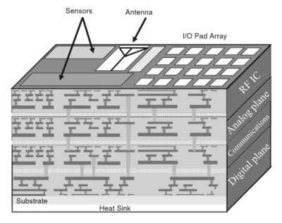
Recently, rumors and educated guesses coming from silicon insiders have pointed towards true three-dimensional chips as the future of the industry. These chips aren’t a few layers thick like the example above. Instead of just a few dozen layers, 100 or more layers of transistors will be crammed into a single piece of silicon. The reasons for this transition range from shortening the distance signals must travel, reducing resistance (and therefore heat), and optimizing performance and power in a single design.
The ideas that are influencing the current generation of three-dimensional chips aren’t new; these concepts have been around since the beginnings of the semiconductor industry. What is new is how these devices will eventually make it to market, the challenges currently being faced at Intel and other semiconductor companies, and what it will mean for a generation of chips several years down the road.
The History of 3D Chips
In the late 1960s and early 1970s, chips became increasingly complex. The forefront of semiconductor technology moved from op-amps and small digital packages to semiconductors with thousands of transistors, and with this came in increasing reliance on interconnects between different portions of these chips.
In the march of technology over the past fifty years, transistors have gone from something you can see with the human eye to tiny specks only a few atoms wide. Interconnects become the dominant design choice, especially with ever-increasing complexity of designs, increasing bus width, and more numerous inputs and outputs.
Because all but the most basic integrated circuits are inherently three-dimensional, the obvious choice for where to put these interconnects was the same solution in any sprawling metropolis; if you can’t grow out, grow up.
This line of research continued throughout the 1970s, 1980s, and 1990s as an academic pursuit, with solutions to new problems. How do you cool the inside of a cube? You can put cooling channels throughout the entire chip. While these problems were simple to define, and the solutions easy to explain, taking the entire idea through manufacturing to a finished product was hard. A much easier way to increase transistor density was to stack individual packages on top of each other.
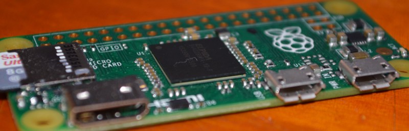
These Package on Package devices can be seen – albeit at an oblique angle – on dozens of devices. The large chip on the Raspberry Pi Zero, Model A, and Model B are POP devices, with the RAM on the top chip connected directly to the Broadcom CPU. The latest, highest capacity RAM modules also use this technique. The JEDEC standards for memory don’t account for 16GB DDR3 modules, but that doesn’t mean you can’t buy them. Here, again, PoP devices are how companies are getting around the problems of interconnects.
The Current State of 3D Chips
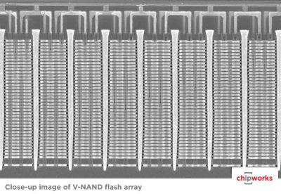
Chipworks did a terrific teardown of Samsung’s V-NAND found in Samsung’s 850 Pro SSDs. It is, by any measure, an incredible feat of engineering. The V-NAND stack found in these SSDs are a 38-layer sandwich of transistors, with each transistor holding one bit of information.
This innovation obviously allows Samsung to put more transistors into a small area, leading to higher capacities. If you believe the Samsung marketing material, up to 100 layers of transistors can be stuffed onto a chip, paving the way for very, very high-capacity drives. This capacity isn’t the only benefit; thanks to the construction of V-NAND, interference between memory cells is reduced, making the drive more power efficient. Write endurance – the number of times a memory cell can be written to without going bad – is improved over normal 2D NAND Flash.
 Even if most of the claims about Samsung’s V-NAND 3D Flash technology are marketing wank, you can’t deny it’s a very good SSD. Look on any ‘build suggestion’ thread in the forums of any PC-based community, and you’ll find a Samsung 850 Pro SSD somewhere in the parts list. 3D Flash is a technological triumph and a market success. The question on everyone’s mind then becomes ‘when is it going to be more than just SSDs?’
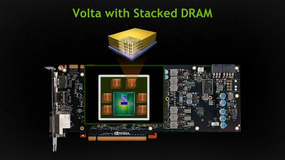
The next generation of Nvidia GPUs, Volta, will feature stacked DRAM when it is released in 2018. While this is about the same level of complexity as stacked NAND Flash, it does tell us that 3D chips are hitting the mainstream, and it’s only a matter of time before we can think of a CPU as a true 3D device, and not just a few layers placed on top of each other.
3D CPUs
If you trace the origins of interesting technological achievements in semiconductors, the usual progression begins with universities, moves into production with memories, and finally becomes part of the glue that holds CPUs together. At one time, Intel was best known for their very high-capacity DRAM chips (hundreds of bytes!), before the knowledge gained in their manufacture moved over to CPUs.
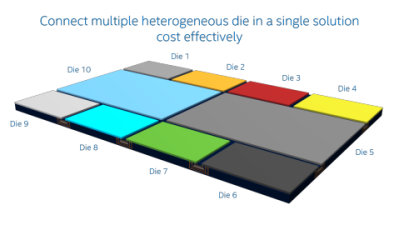
While putting multiple dies on a single piece of silicon will be a boon for Intel – especially with the Altera IP in their portfolio – it’s not exactly a true three-dimensional chip. That will have to wait a while; we’ve only had 3D Flash for a few years now, and 3D RAM won’t be public for another two years. Making a 3D CPU is a much more complex engineering challenge, and for that we may be waiting the better part of a decade.
Three dimensional chips will be released, though. It’s only a matter of time. There’s simply no other way to increase the density of interconnects, the number of devices on a chip, or speed than by moving into a third dimension of silicon.


‘Silicon wafer’ not ‘silicone wafer’ – silicones are polymers, silicon is a pure element.
Comment trap. You fell for it.
I actually believe you. lmfao.
Great to see this topic on Hackaday!
However, the omission of silicon interposers and through-silicon vias is a disgrace! Multiple companies are shipping 3D-stacked silicon dies, including HBM memory which you describe as “won’t be public for another two years”. Samsung, Intel and Nvidia are far from being leaders on this field.
Next stop: Computronium
That relies heavily on Unobtainium.
And Wonderflonium.
Cooled with Immatereon
Encased in Scrith.
and with a lemmium power supply.
Improbolium inside
Shouldn´t there be some kind of info that the title image was taken from Tron (1982)?
The featured and thumbnail images were created by our illustrator, Joe Kim. You can find his work here. It looks more like Moses from South Park, anyway.
Oh, I´m sorry then. It really loked like from the movie.
But honestly, it looks more like MCP than Moses.
Not sure if Moses would fit in with a 3D bars and pipe screen saver…
Wow. His work is awesome.
Thanks Brian, I always wanted to ask who is this fantastic artists.
I check hackaday.com partly of the possible new graphics.
Came here to agree, it totally looks like South Park’s depiction of Moses.
So he also designed the evil Tron A.I. in 1982?
https://brianwelk.files.wordpress.com/2012/11/mcp1.jpg
Or is his artwork the addition of the pipes?
We’ll gladly update you if and when Disney sues us.
You must looove C&D orders, lol.
I don’t understand why the article talk about Nvidia that will have something in 2018, while AMD already have stacked DRAM memory since half a year.
http://www.amd.com/en-us/innovations/software-technologies/hbm
https://en.wikipedia.org/wiki/High_Bandwidth_Memory
exactly
why cite Nvidia, when AMD was the one developing this tech and actually has shipped product
nvidia on the other hand claimed Pascal would have HMB – it wont, and then later LIED TO PRESS claiming to have taped out 16nm GPUs already
http://semiaccurate.com/2016/01/11/nvidia-pascal-over-a-year-ahead-of-1416nm-competition/
Yup, exactly what I was going to say. Proof that Hackaday “journalists” do little to no research on what they’re writing about. Not even a quick google…
Maybe you shouldn’t read hackaday for journalism, then. If I want research, and all the technical references that go with it, there are other blogs to read; mostly directly from various college research groups. That’s not the reason to read, the tip-line, the community, the hacks and maker stuff is what makes it worth reading.
But go ahead and keep reading while complaining about everything that doesn’t fit your ideal. You could offer to make it better, like jcamdr who pointed out more information; but “ditto”ing that with snark is easier I guess.
I disagree. When someone write a text about “The Current State of 3D Chips”, readers expect that the author do at least some very basic checks as Fennec try to say with his own words.
The author talk about JEDEC standard, so it’s logical to talk about the JEDEC standard for HBM stacked DRAM that exist since 2013 and is _currently_ in production for AMD GPU. AMD was working on this technology since 2008, so it logically take place in the article.
Even if you don’t like some reactions, there are perfectly legitime for a such simple error. There are sometimes more comments about far more futil issue. And what’s the purpose of your specific comment anyway ? You don’t provides more informations as you recommend for example.
There’s no pleasing you is there?
“Not a hack.”
“The site is called ‘Hack a Day’, so you’re only entitled to one hack per day, and the editorials are very informative.”
“This article isn’t very well researched.”
“Well-researched editorial articles aren’t what we come to HaD for, it’s the hacks.”
…just as I’m sure you’d have absolutely no objection to a compendium titled “Life on Planet Earth” that somehow neglected to mention that anything more complex than amoebas actually exists here. Right, next White Knight please…
I’m making fun of the white-knights.
Also, I was pointing out a bit of hypocrisy.
Yield has to take a hit though. I’d assume doubling the number of layers would double your failure rate.
I think you mean the success rate would square for each doubling of layers?
Squaring, yeah, that would make more sense. But counting success rate vs failure rate depends on how you measure. Wolfram Alpha does the strange math of (50%)^2 being (50^2)/100, since percent means “per hundred”. That would take a 50% success rate up to 2500% when squared.
Maybe it’s because it’s not treating percentage as a hard figure but more like a different way of writing a multiplier.
Not necessarily. The really important thing when stacking things is that each layer is flat, if one can make each additional layer flat then the errors per layer will not increase by much. It will cost a lot of money of course so the 1000+ layer chip is far away in the future (if ever). However using 3D stacking also makes using less costly lithography possible, e.g. using 28nm per layer with 4 logic layers is potentially more useful and much cheaper than doing a 7nm chip with one logic layer.
( This is extremely simplified – the quality one can deposit each new silicon layer is another very important aspect for errors, performance and heat production, the quality of the VIAs is another. The whole thing is much more complex than rocket science :) )
Although reducing the distance that signals have to travel will reduce path resistance and thus heat, I would think that the heat generated by transistors as they switch will be orders of magnitude greater. The advantage of 2D chips is that you can build the whole thing on a heatsink. When you bury transistors deep into a block of silicon, getting the heat out will be a lot more difficult (and will require it to pass through other transistors on the way). It will be interesting to see how this problem is addressed (I’m sure that they are working on it)
They won’t. That’s why the technique is being applied to RAM and Flash first: lower active power demand.
The ideas to cool a 1000 layer CPU mostly involve sacrificing most of the transistor density by punching holes with some sort of volatile liquid through them. so the chip would be inside a heatpipe much like how the Cray supercomputers were designed with fluorinert flowing through and between the circuit boards.
The obvious problem is that there will be detritus that gets stuck in the tiny channels and the CPU overheats and dies.
I’d think for CPU’s you’d put the heavily active stuff on the bottom by the heatsink, put your low power stuff on the top layers. Even if you only did two layers, and you were able to use the entire area of the bottom layer for the cores and put the cache and other ram components on the full top layer (maybe an in between layer for routing), you could significantly improve your processor without adding too much heat insulation.
perhaps this will spur more research into thermodynamically reversible computing?
Put in 42, add lots of heat and obtain 6*7
Maybe they will do it like they do with drill batteries.
Perhaps they will drill holes and channels through the chip and pump/suck something cold through them.
sure one can increase bounding area of a given volume, but volume will still scale as the cube of a length, and area only as a square… channels are just a temporary hack (a constant factor of improvement, not something that can address the square vs cube).
Maybe you can put the large last-lavel caches in few layers in the bottom, then increasingly power-dense stuff higher up. Not much “3d”, but with 4-8 layers you get 4-8 times as many chips out of a die. Modern cpus has hot spots in that are much power dense the the chip average as it is.
And a lot of the pop-chips in mobile phones etc manage thermally even with a slab of dram on top, so they could potentially manage even in a stack of logic.
“marketing wank”. As a Brit that’s a new one on me! I thinks Mr Benchoff likes British “-isms”.
It has different implications in American English:
http://catb.org/jargon/html/W/wank.html
That page is very strange to read with the meaning known by this American English speaker.
There are ongoing discussions about adding graphene heat pipes inside the silicon, as vertical towers.
Why waste time using graphene as the heat pipe? Lots of progress has been made using graphene directly as the conducting layer. With such a low resistance, little heat would be generated and no need for heat extraction. It’s just better efficiency. Also, layers at one atom thick means more stacking in the same cubed area as silicon. I am skeptical of graphene from its useful applications, however integrated circuits seems to be its solid future. Battery technology improved with graphene would be great, but very little progress is being made there and nothing but hype is being generated.
Using graphene as conductors (something that is still theoretical, changing interconnect materials are a very complex task) wouldn’t significantly reduce heating on the chip. Transistors have both a fixed leakage current and a variable switch-activity dependent current and graphene interconnects would not directly affect those. Sure it would help as the reduced RC delay etc. also affects the transistor sizing but there still would be a lot of heat that have to be transferred away for the devices to work.
Even if with current state of the art technology the costs of higher layer counts would not yet be offset by performance gains, it may be offset by infosec considerations, as inspecting high layercount chips could be substantially more difficult.
I remember back in the mid ’70 and I was working at Fairchild R&D, (then chairman) Lester Hogan announced a design for 3D memory.. as far as I know it never left the design sheet.. but it was fun to think about.. IBM Almaden also did some seminal work on this in the mid ’90s..
I saw the title and immediately thought of the Raspberry Pi’s PoP RAM arrangement. Such a thing is 3D only in the sense that the average office building is 3D, which is to say… not so much. An office building is really a stacked arrangement of 1 story sub-buildings. The only logical connections between them are “service busses” which supply utilities and human ingress/egress between each and the entry point for the structure.
The next level of abstraction with this idea was the erstwhile World Trade Center in Manhattan. Each of the twin towers was made of three individual hundred-story office buildings vertically stacked. At the base of the second and third was a “sky lobby” that one accessed via express elevator from the ground floor. One then transitioned to “local” elevators that were vertically stacked so that the elevator for floors 1-99 used the same vertical space as the ones for 100-199 and 200-299 (in fact, it was a bit more complex, as there were actually separate elevators for 1-33, 34-66 and 67-99, and then separate ones that went from Sky Lobby 1 to 100-133, 134-166 and 167-199 and so on).
But none of that seems like 3D architecture – more like PoP. True 3D architecture would have been more like the Winchester Mystery House, which has all sorts of interconnections between the two stories to make inter-floor relationships much more widespread. It’s the kind of thing that even today is quite rare.
Ok, I went back and checked… Divide all the numbers in that comment by 3 (except where it says “3D”). :)
The ultimate in 3D chips would work like this,
It would be made of graphene in the form of a Minimal Surface (array) or even nested surfaces,
http://www.pa.msu.edu/people/tomanek/GNJ/SI/periodic-minimal-surface/index.html
Except that slots and holes are punched out of the surface because the exact form of the edge structures allow you to form areas that vary from superconductor to semiconductor to insulator, with no other elements involved.
You can build an optimal circuit just by arranging the connections of carbon atoms and the relationships between layers, but if you do dope it you have even more options. The doping falls into two categories, changing areas to change electrical properties and changing areas to induce changes in curvature to cause the minimal surface/s to assemble.
See:
http://link.springer.com/article/10.1007%2Fs12274-014-0611-z
https://books.google.com.au/books?id=2Ku9BAAAQBAJ
http://www.innovationtoronto.com/2015/12/123819/
http://physicsforme.com/2011/05/28/how-to-make-graphene-superconducting/
http://phys.org/news/2015-04-holes-graphene-energy-storage-capacity.html
https://physics.aps.org/articles/v3/46
http://what-when-how.com/nanoscience-and-nanotechnology/fullerenes-topology-and-structure-part-1-nanotechnology/
The only reason we can’t do this right now is the fabrications methods are not mature enough, even if all the basic steps have been demonstrated in the lab.
Why would graphene be better in such a design than the already known and used niobium? If one want to use superconducting logic then the way to do true 3D designs with niobium is already known – what is missing is the effort to improve the manufacturing processes.
Superconducting logic is a better match to 3D stacking due to much lowered heating effects, the fact that the logic layer is the same (or can be made the same) as the metal routing layers etc. The problem is the cooling.
You can self assemble graphene minimal surfaces using biochemistry. Take the metabolic pathways that make https://en.wikipedia.org/wiki/Hypericin and change them to have the R groups encode for this behaviour. http://www.logarithmic.net/ghost.xhtml?bbBBbB&bbBbBB I’m not going to tell you how to do everything but that is the direction you need to look.
Once your computing device has self assembled you can have a inert liquefied gas flow through the structure if you need cooling. The minimal surface is more than 2D and less than 3D so you can nest them and still have paths through then entire assembly for cooling, or for photons to travel through. So yet you get an optical interface and interconnects for free. Remember those patches of semi-conducting graphene….
Sorry about the typos, and I forgot to mention that Ghost Diagrams are Turing complete so they can construct any pattern. They are not limited to 2D either. So the right codes will create any target pattern. http://www.logarithmic.net/pfh/blog/01104447019 So the trick is to work back from the patter you need to the code that produces it, a non-trivial task, but the sort that quantum computers may be idea for solving.
They are going to need to figure out substrates for this to work, for thermal exfiltration.
The ideal solution would be a cheap and fast way to make insulation between layers out of monocrystalline diamond. But then anti-gravity would be a cool thing too! ;)
I somehow omitted a word there … the most important word …. which you pointed out: diamond.
Anyhow … if they use diamond substrates and then stack those, they’ll get the desired cooling effect.