It is something of a rite of passage for an electronics enthusiast, the acquisition of a first oscilloscope. In decades past that usually meant a relatively modest instrument, maybe a 20MHz bandwidth and dual trace if you were lucky. Higher spec devices were eye-wateringly expensive monsters, not for the Common People.
We are fortunate that like most other areas of technology the world of test equipment has benefited in the last few years both from developments in digital technology and from the growth in Chinese manufacturing. If your first ‘scope is that second-hand 20MHz CRT you will probably secure it for pennies, and the first ‘scope you buy new will probably have a spec closer to those unattainable super-scopes of yesteryear. Gone is the CRT and timebase generator, in its place a TFT, system-on-chip, and super-fast A to D converter.
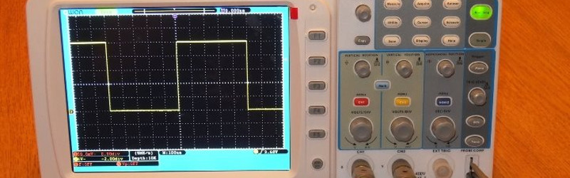
[Christer Weinigel] has just such an entry-level modern digital ‘scope, an OWON SDS7102. He comments that it’s got an impressive spec for its price, though the input is noisier than you’d expect on a more expensive device, and the software has one or two annoying bugs. Having owned it for a while, he’s now subjected it to a lengthy teardown and reverse engineer, and he’s posted his findings in a succession of blog posts.
[Christer]’s interest lay mainly in the OWON’s digital section, it seems there is already a substantial community paying attention to its analog front end. He’s deduced how its internals are connected, ported Linux to its Samsung SoC in the scope, succeeded in getting its peripherals working, and set to work programming the Xilinx FPGA that’s responsible for signal processing.
The series of posts is a fascinating read as a run through the process of reverse engineering , but he points out that it’s quite a lot of information. If you are just interested in how a cheap modern oscilloscope works, he says, he suggests reading his post in which he recaps on all its different components.
He also makes a plea for help, he’s no slouch on the ‘scope’s software but admits he’s a bit out of his depth on some aspects of the FPGA. If you’re an FPGA wizard with an interest in ‘scopes, he’d like to hear from you.
This isn’t the first time we’ve featured ‘scope reverse engineering here at Hackaday, though it may be more in-depth than others. In the past we’ve seen a Uni-T screen grab protocol laid bare, and an investigation of a Rigol 1054Z.


‘scope creep
Amazing work. Just a shame that they can’t be much improved anyway due to processing and hardware limits. Usually all the reverse engineering just leads to something similar than what was there already.
Amazing excellent work! Please continue!
Jeezus this is amazing.
Is it possible that the fpga->ddr2 memory interface goes the other way? Ie, you halt the CPU, use the FPGAs memory controller to write the trace data to a location in ram, then resume the CPU and read the data out of ram? I have only seen this approach done with dual port ram (so you do not need to halt the CPU while writing) but it seems like it would work… Certainly be easier to implement than building a ddr2 emulation core.
since the 2 ddr2 memories are of the same type according to his write-up, I would suspect instead that they are used in a “double buffering + swap” setup, i.e. repeatedly:
ADC -> mem1 while mem2->SoC then swap
ADC -> mem2 while mem1->SoC then swap
The reverse engineering from the software and FPGA bitstream sides is stunning. Nice work. I really want to see all the gory details of the analog signal path including all the bits driving the ADC, clocking etc. But, I have a particular reason for this as part of my current project research. The FPGA stuff is not so hard(for me) but I admit, using the DDR2 interface on the SoC for the FPGA interconnect is pretty hardcore – I suspect the bandwidth through the simpler interfaces was not sufficient. It’s not like the Chinese to take the hard route just for the fun of it :D
I’m not really sure why they went with the DDR2 interface. As you say, it has higher bandwidth (133MHz * 16 bits for the DDR bus instead of 67MHz * 16 bits for the peripheral bus) on the other hand the FPGA has to compete with the DDR memory for bandwidth. The DDR memory interface is also much more complex: instead of a read being a simple “here’s the address, give me the data” the CPU now has to do a precharge to open a memory row, read from the row and close the row; all this costs latency.
I could imagine some the Owon having tricks in mind like letting the display controller in the SoC render graphics from the virtual DDR memory in the FPGA. That would probably not work if the FPGA is connected to the peripheral bus. Displaying data directly from the FPGA that might allow some really nice “virtual phosphor” effects that would not be possible otherwise. On the other hand, the peripheral bus could be used to do DMA directly from the FPGA to the SoC main memory and that ought to be enough to let the FPGA update the display at 60Hz.
It might be that the Owon engeineers having done a virtual DDR2 memory before and that is is a case of “if all you have is a hammer, everything looks like a nail”. Who knows. :-)
I’m guessing they’re using the LCD controller’s layer feature to composite the CPU-rendered UI bitmap with an FPGA-generated waveform bitmap.
From Weinigel’s first blog post:
“…There is a huge thread discussing the SDS7102 on EEVblog forums and other people has [sic] done quite a bit of reverse engineering of it already. They have mostly concentrated on the analog parts and I’m more interested in the digital parts and the firmware…”
Not “one of the…”, but THE most important part of an oscilloscope is the analog front end.
The hardest part of problem-solving is to identify the correct problem.
Doing a 100MHz analog frontend is pretty much a solved issue today. Throw money at it and use a one chip variable gain amplifier with enough bandwidth, or cost optimize and do it with discrete component as the Rigol 1054Z. What actually differentiates most 100MHz/1Gsample/s scopes today is the signal processing and software.
And my goal is to see what the existing SDS7102 hardware can do. For _me_ the AFE isn’t that interesting, I’ll have to make do with whatever is in the scope already, I don’t care if they use a Chebyshev filter or a Butterworth filter, I care if changing an I/O pin on the SoC changes the attenuation and by how much. Yes, reverse engineering the analog circuits of the AFE is one way of figuring out what an I/O pin does, another way is to treat the AFE as a black box and just switch the I/O pin and see how it affects the signal seen at the ADC.
And the problem he wanted to tackle was the buggy firmware. He isn’t trying to fix analog issues.
And his reply popped up after I posted mine, even though he posted long before me. Oh well.
And just for fun. I can live with the buggy firmware, the scope is still useful as is, but well, I’m a nerd.
Christian,
I went thru your blog. Even not understanding most of it, it was pleasure to see how talented hackers utilize their skills.
really impressive and good luck with further work.
Best regards from .PL
ups , your name is Christer .. sorry for that… :)
No problem. I’m used to it. It took my best friend a while to learn to say Christer instead of Christian. :-)
From your findings is seems unmitigated NAND Flash wear/corruption amounts to either “Planned Obsolescence” if not outright incompetence. Thank you Christopher for your investigation. OWON is now at the bottom of the ladder for me when I consider test equipment.
I’ve seen a few posts by people who can no longer boot their SDS7102 scopes but most of them seem to be due to a failed firmware update. I don’t think I’ve seen anyone who has had a scope fail just by doing nothing. There are probably lots of other products based on Samsung SoC that have crappy bootloaders and don’t use error correction.
I would personally not feel comfortable about having a product in the field which doesn’t use error correction for the NAND flash, but I might be overly paranoid. :-)
I’ve managed to capture samples from the ADC now:
http://blog.weinigel.se/2016/07/08/sds7102-capture.html
I still have no idea where to start on the SoC->FPGA bus or the FPGA DDR memory.
And a bit more. I repurposed the ADC capture to take a look at the SoC bus.
http://blog.weinigel.se/2016/07/10/sds7102-soc-bus.html
One final post. Or not.
Anyway, with this I have basically documented how everything in the scope fits together.
http://blog.weinigel.se/2016/07/15/sds7102-afe.html
If you aren’t bored with me yet.
I’ve put the source code for my Linux port and FPGA image on github.
http://blog.weinigel.se/2016/07/16/sds7102-source.html
I’m not sure if anyone is still reading the comments here, but…
I’m on vacation and the weather isn’t too nice so I’ve spent waay to much time hacking on my FPGA image. I’ve now managed to make the emulated DDR2 memory on the SoC bus read/write and can capture data from the ADC directly into the DDR2 memory attached to the scope.
http://blog.weinigel.se/2016/08/15/sds7102-ddr-capture.html