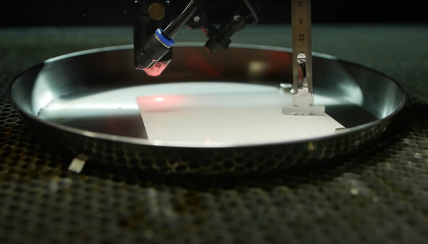
[Ben Krasnow] over at Applied Science was experimenting with cutting inexpensive ceramic sheets with his cheap CO2 laser cutter when he found that (just as expected) the thermal shock of the CO2 beam would cause cracking and breaking of the workpiece. After much experimentation, he stumbled upon a simple solution: submersion under a thin layer of water was sufficient to remove excess heat, keeping thermal shock at bay, and eventually cutting the material. Some prior art was uncovered, which we believe is this PHD thesis (PDF) from Manchester University in the UK. This is a great read for anyone wanting to dig into this technique a little deeper.
The CO2 laser cutter is a very versatile tool, capable of cutting and etching a wide range of materials, many of natural origin, such as cardboard, leather and wood, as well as certain plastics and other synthetic materials. But, there are also materials that are generally a no-go, such as metals, ceramics and anything that does not absorb the laser wavelength adequately or is too reflective, so having another string in one’s bow is a good thing. After all, not everyone has access to a fibre laser.
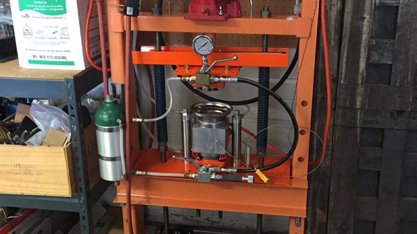
After dispensing with the problem of how to cut ceramic, it got even more interesting. He proceeded to deposit conductive traces sufficiently robust to solder to. A mask was made from vinyl sheet and a squeegee used to deposit a thick layer of silver and glass particles 1 um or less in size. This was then sintered in a small kiln, which was controlled with a Raspberry Pi running PicoReFlow, and after a little bit of scrubbing, the surface resistance was a very usable 2 mΩ/square. Holes cut with the laser, together with some silver material being pushed through with the squeegee formed through holes with no additional effort. That’s pretty neat!
Some solder paste and parts were added to the demo board, and with an added flare for no real reason other than he could, reflowed by simply applying power direct to the board. A heater trace had been applied to the bottom surface, rendering the board capable of self-reflowing. Now that is cool!
Continue reading “Water Is The Secret Ingredient When Laser Cutting Ceramics To Make Circuits”