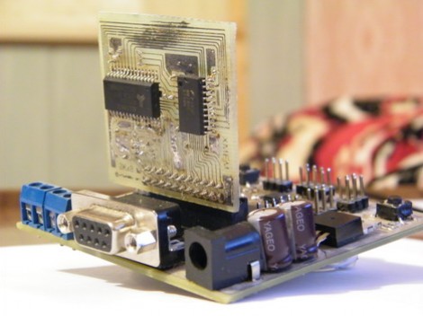
Those who are familiar with Atmel’s line of 8-bit AVR microcontrollers should already know that some of them have support for external RAM. But have you ever actually used this feature? We haven’t. Now you can learn how it’s done by reading through this guide. It touches on all of the hardware, but doesn’t dwell on it. Instead, you’ll get the background you need on how to write to, read from, and test an external module like the one sticking up in the image above. The test routine shows how to make sure everything’s working correctly with your memory mapping before you begin developing firmware around this increased capacity.
[Thanks Spman]


Great work!
i can find a couple of uses for this
like have it record a vast amount of data really quickly than throw it in an SD card after
This could also be used as a memory-mapped FPGA interface.
Obligatory post about how this is what Hack a Day has ‘come to’.
Two weeks ago, this would have been of great use to me. Oh well, better late than never.
Is it bad that the first thing I noticed were the Yageo electrolytic caps, and that my first reaction thereto was “ew”?
Anyway, that’s seriously awesome, not least because it’s reminiscent of the computers of yesteryear, when a few hundred KB of RAM came on boards not a lot different from that one.
Add an avr->teleprinter interface, and you’re well on the way to early 1970s computing power. :)
@George
Not exactly. The AVR can be run at 20MHz, while your ’70s era machines tended to be a third of that, perhaps less.
However, I thought about that as well. Not just because of the memory, but because of the size of the memory board.
@MissingFrame: Can you expand on that comment? I don’t understand what you mean but I’m interested.
As long as we’re thinking retro, instead of just expanding the RAM to something you’d find built-in on a better MCU; why not add a few extra I/O lines and bank switch for 128KB or more? ;)
Great work! You can NEVER have enuff RAM! And if you don’t mind a bit of an ugly soldering hack, a 512K SRAM is easy to hang on an AVR without a PCB…
http://www.lucidscience.com/pro-vga%20video%20generator-1.aspx
Cheers!
Brad
Sorry, meant to link to the photo of the 512K SRAM here…
http://www.lucidscience.com/projects/VGA%20Video%20Generator/24.jpg
Brad
Nice! I wish it was this straightforward to interface 32bits wide memory.
>Obligatory post about how this is what Hack a Day has ‘come to’.
hahaha obligatory “not a hack” post :P
on topic – looks very cool :)
thank GOD that is not arduino up there in the picture
:)
@Mike Szczys
Accesses to external memory are well documented in the datasheet. In short, the MCU puts out the address value and a “read” signal; or, in case of writes, the address&data values and a “write” signal. FPGAs, CPLDs, even discrete logic can decode the address and map it to some function.
For example, a few additional “remote” I/O ports :) — a nice addition when the external bus has consumed all native I/Os but there’s plenty of pins and memory remaining on the FPGA.
Another example: a simple discrete address decoder is everything an external UART (16550A clone) needs. It has 8 internal registers that are addressed by 3 pins A0…A2. The decoder must compare A15…A3 of the external bus with some constant and route that to an appropriate “chip select” pin of the UART. A0…A2, RD, WR from the MCU can be used directly. This way all reads/writes at addresses base+0…base+7 will go to the UART.
Of course this calls for a tutorial. Sadly I don’t have that custom-made development board anymore, and a bare theory is barely convincing.
@Mike Szczys
saimhe did a great job of explaining it. Really if you only need more RAM on a small MCU, you’d just get a bigger part. What this enables is the more open memory-mapped I/O architecture of the typical 8 bit computers of yesteryear.
I guess I was a few steps ahead in those thoughts, when creating FPGA interface to an MCU, it can be very efficient to have it look like SRAM. Especially sometimes if you have an actual SRAM buffer in the FPGA.
Yeah, a project I’ve been thinking of would memory map the BRAMs of a Xilinx Spartan such that it would appear as external memory to a USB AVR.
This would permit a multi-universe USB-to-DMX adapter with good performance – Basically take incoming data from USB, dump it in the “external RAM” (really mem-mapped FPGA BRAMs), and hardware in the FPGA would send every 512 bytes as a DMX universe on one output pin.
You could probably have 8-16 universes with good refresh rates without any I/O bottlenecks.
Unfortunately, the USB AVRs that support XRAM don’t have many good boards based on them. Most people that offer USB AVR boards are offering smaller devices (like the 32U4) or have done something to make the XRAM interface unworkable.
char some_buffer[256] __attribute__ ((section (“.noinit”)));
Network debug output FIFOs, socket FIFOs, audio playback FIFOs, event log buffer, SD card write buffers… the big stuff mainly since you don’t want to put so many attributes in the code.
As other’s have said this is more interesting for memory mapped peripherals than just attaching SRAM.
With a few GPIO pins for chip selects or some address decoding logic you can attach external peripherals with a nice fat databus. You could for instance drive some of the RTL network interface chips, programmable sound generators.. if you really want you could probably get an ISA interface working and drive old school sound and graphics cards.
Oh, forgot something.. there’s nothing to stop you wiring up on of those SRAM + Battery NVRAM blocks either.. or maybe a FRAM.