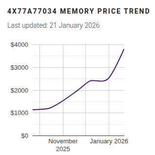
DDR3 seemed plenty fast when it first showed up 19 years ago. Who could say no to 6400 Mb/s transfer speeds? Of course compared to the modern DDR5 that’s glacially slow, but given that RAM is worth its weight in gold these days– with even DDR4 spiking in price– some people, like [Gheeotine], are asking “can you game on DDR3“? The answer is a shocking yes.
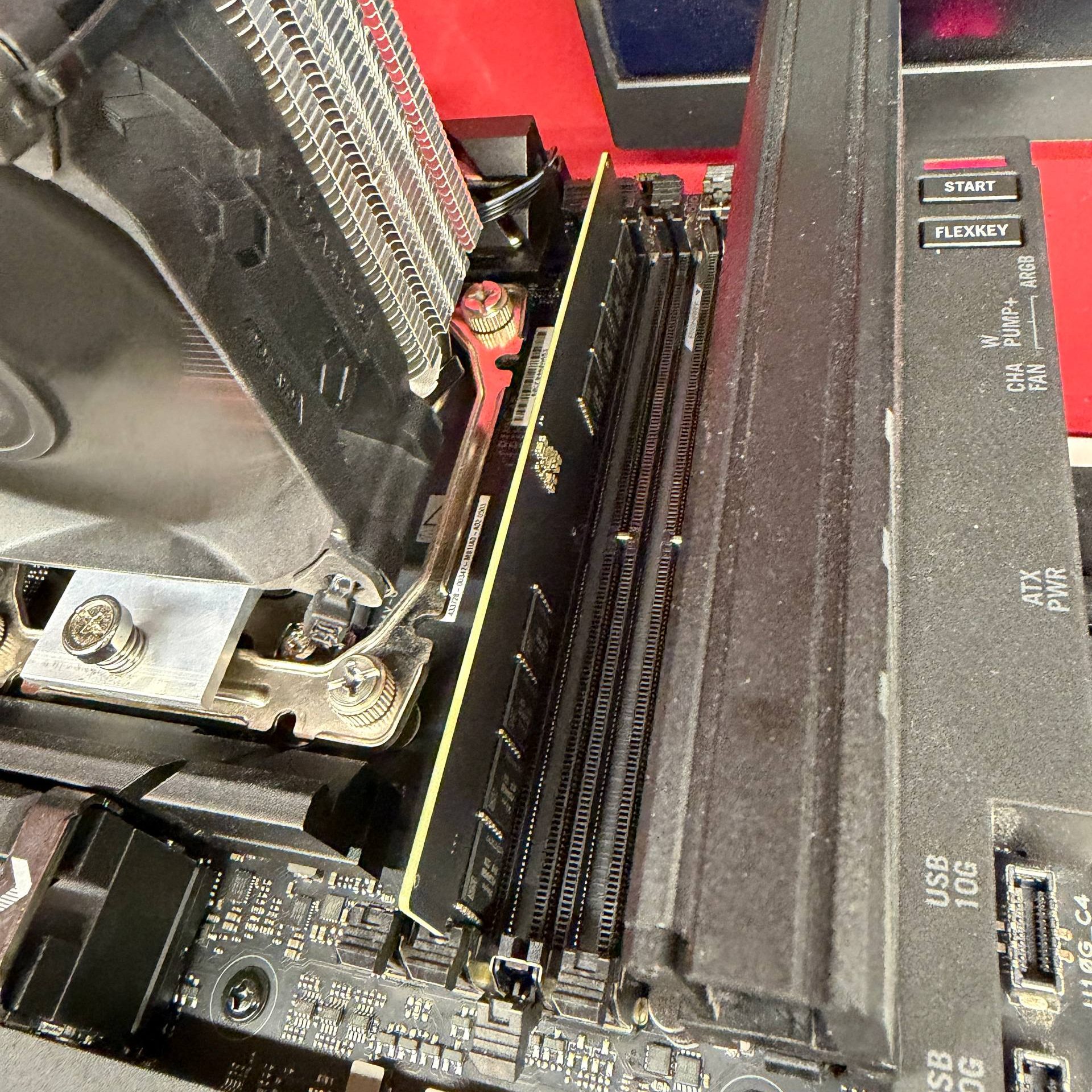
[Gheeotine] builds two budget-friendly PCs for this video, using some of the newest DD3-supporting motherboards available. That’s not exactly new: we’re talking 12 to 15 years old, but hey, not old enough to drive. We certainly didn’t expect to hear about an x79 motherboard hosting an Ivy Bridge processor in 2026, but needs must when the devil dances. The only concession to modernity is the graphics cards: the x79 mobo got an RX6600XT 8GB, and the other build, using a z97 motherboard got an NVIDIA RTX 4060. The z97 motherboard allowed a slightly newer processor, as well, an i7 4790, with the new and exciting Haswell architecture you may have heard of. Both boards are maxed out on RAM, because at less than one USD/GB, why not?
[Gheeotine] puts a few new titles through their paces on these boxen, and while the results aren’t amazing, everything he tries comes out playable, which is amazing in and of itself. Well, playable unless you’re one of those people who can’t stand playing at resolutions under 4K or FPS under 100. Those of who spent their formative years with 29.7 FPS or 25 FPS in NTSC or PAL regions aren’t going to complain too loudly if frame rates dip down into the 30s playing at 1080p for some of the more demanding titles. Ironically, one of those was the five-year-old Crysis Remastered. Given the age of some of this hardware “Can it Run Crysis” is a perfectly reasonable question, and the answer is still yes.
If you want modern games, you’re much better off with a z97 chipset motherboard if you chose to go the DDR3 route, since you won’t run into issues related to the AVX2 instruction, which first appeared with the Haswell microarchitecture. Here at Hackaday our preferred solution to the rampocalypse is software optimization, Since holding your breath for that would probably be fatal, cost-optimizing PC builds is probably a good plan, even if some might balk at going all the way back to DDR3.
Of course if you’re going to use nearly-retro hardware like DDR3, you might as well go all-out on retro vibes with a nostalgic 80s-style, or even 50s-style case.
Continue reading “RAM Prices Got You Down? Try DDR3. Seriously!” →