If you’ve got an ARM development board gathering dust in the corner of your shop, perhaps you could repurpose it as an oscilloscope. [Arend-Paul Spijkerman] was able to use an mbed and LPCXpresso as the hardware end of an oscilloscope. He didn’t use a standalone screen as a display, instead opting to push the scope readings from the hardware to a computer for display. This was greatly simplified by using StampDock as a basis for the GUI.
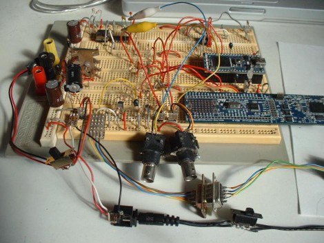
His circuit diagrams calls for an RS-232 connection for the LPCXpresso but not for the mbed. We’re not quite familiar enough with the mbed to know why, but perhaps those in the know can clue us in by leaving a comment. The probe connections are quite simple, each made up of a voltage divider and a pair of diodes. But the breadboard above looks much busier because it has two oscilloscope circuits built on it, and there’s a 10 MHz clock and a 4040 ripple counter which were used to provide a test signal.


@creator
Whats the max freq of the lpc this can operate? I’d be willing to build this as a “plug in” to the lpc once I put some male/female headers on it
Hmm this might me a good alternative to buying a expensive one. Been wanting one for awhile except for the cost.
Agreed. Though those inexpensive little DSO Quad scopes are probably a good way to go if you don’t already have hw around.
Is there a link to more details?
i love my LPCxpresso
some more info: http://apsdev.com/stampscope2/home.html
@MikeSzczys: The mbed supports a virtual serial port over the USB along with using it for programming which I’m guessing that they used instead of adding an extra port.
@Mike: I thought it had been missed but the details can be found after the StampDock link
Sampling speed?
Here is the link.
http://apsdev.com/stampscope/home.html
Uses LM324 on the input. LM324 have a unity gain bandwidth of 1 MHz. Looks audio to me.
maybe we can build a pcb. i have my lpcxpresso here next to me ready.
It can be used one of this display modules. I made an simple app but it can be optimized far more http://www.youtube.com/watch?v=-488Nk1t9kQ
The LPCXpresso has an LPC1114 microcontroller, which as a 10-bit ADC. The data sheet says the conversion time is at least 2.44 µs (section 7.11.1). If samples were taken each 2.44 µs, that results in a sampling rate of about 410 kHz. Not great, but still very useful for many tasks. Although… in footnotes on Table 8 (LPC111x Data Sheet, Rev. 2, p. 33), it says “maximum sampling frequency fs = 4.5 MHz and analog input capacitance Cia = 1 pF.” I don’t understand how the sampling frequency can be 4.5 MHz if the conversion time is at least 2.44 µs. The input impedance of the ADC looks decent, around 2.4 Mohms.
ColinB, as I understand it, the max fs of 4.5 MHz is the ADC clock, not the sample rate. A conversion of N bits takes (N+1) ADC clock cycles (it uses successive approximation). So for 10-bit data you can do 4.5M/11cycles = 409 kS/s. If you require less bits, it can go a little faster, for example 8-bit conversion can go at max 4.5M/9cycles = 500 kS/s theoretically.
Note that as you can change the MCU code and the GUI layout it is more or less an open source instrument.
Which means by some simple edits in the code you can add more channels, as the chips have more then 2 analog inputs.
Or if you have a fast ADC chip you can add that, and change some lines in the code.
Or with some small changes you can add a logic analyzer mode or make a spectrum analyzer or wobler. The only limit is which LPC chip you use.
Thats the point of the stampdock software .. you can use it as a univeral GUI for MCUs.
You could even change it into something completely different, like a signal generator.
Greetings APS..
Whats the mbed for in this project?
so. . . by extension, if you had a better ADC chip, an RS232 chip, and that schem, would you really need any other function of the uC? (signal generator, oscilloscope etc?) or is the uC controlling something that I’m not understanding.
because this could be a step to making a cheap and open source oscilloscope for the student just starting in electrical design
can someone design a pcb for this? i have a lpc expresso.
would like to create a mini huntron using this if it possible