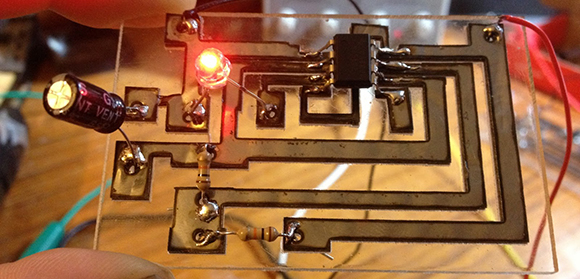
Despite what you may have heard, those 40 Watt laser cutters actually can cut out traces on your next PCB.
Since he got his laser cutter a year and a half ago, [Rich] over at Nothing Labs has been trying to cut PCBs with it. Others have tried, usually by masking off a piece of copper followed by chemical etching. [Rich] wanted a one-step process, though, and his laser cutter really isn’t up to the task of cutting metal.
All that changed when he heard of another maker cutting .001″ thick stainless steel on a similar laser cutter. Stainless steel isn’t solderable, but mild steel is. After finding a very thin piece of mild steel, [Rich] taped it down to a sheet of acrylic, designed a simple 555 blinky LED circuit, and tried out a new technique.
It turns out it is possible to cut very thin steel into circuit traces, and with enough flux to turn them into a functional circuit. As a bonus the resulting circuit looks really cool and a board can be made in mere minutes.
It’s not the thing for very fine work – the minimum trace width [Rich] can get is about 1/16″, but it is a very fast way to prototype a few circuits.
[youtube=http://www.youtube.com/watch?v=OtZQoIheYcc&w=580]


The problem is that if you have enough power to punch through a layer of metal, fiberglass isn’t going to put up much of a fight.
If the plastic underneath is transparent, it shouldn’t put up any fight! Might be that it’s transparent enough to pass through most of the energy, not absorbing enough to heat, warp or melt itself.
I wonder how you’d do this on a larger scale? Glue a whole thin sheet of steel onto some plastic? The glue would need to set transparent, and every sqaure cm would need sticking down. Something to try, maybe, if you’ve a strange kind of need that this method solves.
Sorry, come again? Transparency means no absorption? I’d have to disagree, what with clear poly-carbonate / acrylic being probably one of the most popular laser-cutting materials in the world! The Trotec 30W machine we bought claims to even be able to etch glass, though I’ve yet to try this!
Maybe if you had some materials that were transmissive to near IR (http://www.internationalcrystal.net/ti_sec1.htm), you might get away with it, but using these materials for a PCB substrate would be ridiculous!
Re the power problem, it’s all about energy dissipation. Commercial machines are more than capable of vaporizing the top layer of copper from a FR4 substrate,at scary speeds. One day, I’ll own one of these;
[youtube http://www.youtube.com/watch?v=mzmjGz0_joM&w=560&h=315%5D
A PCB on a Salt block substrate (http://www.deandeluca.com/herbs-and-spices/salt-pepper/salt-plates-and-salt-brick.aspx) would be quite impressive. And also very insane.
@Tom…
OMG my jaw just dropped, and is still hanging!!! That is bad ass!!!!!!!
ACTUALLY…transparency DOES mean no absorption. YOU (Tom) made the assumption of changing the light wavelength from that for CO2 laser (10.6 um) to visible..not the original author (Greenaum).
This is so cool. I’m all for less mess!
It is definitely interesting and looking cool because it’s rather unusual. But I don’t think that it needs to be justified with excuses like being a “fast way to prototype”. It’s a strange way to prototype.
Kudos! This is how a lot of cool projects start: someone finds a neat concept or tries other materials, builds a proof of concept and others tune and build on it.
i wonder what power is needed to vaporize copper from regular pcbs….. there are commercial machines that can do that…
and yes, this is a strange way to prototype. True it is a one step process, but so is milling a pcb.
PCB laser cutting can be done with a laser cutter, it just takes a special type of laser. Check out:
http://www.youtube.com/watch?v=eSStzkYWYFg
http://www.youtube.com/watch?v=PhH05jNyjCk
LPKF makes a line that does this. They’re exorbitant, but they exist.
Yes .. I tried this too … 300Watt at 25m/s. Result:
http://abload.de/img/dscn11437xkrl.jpg
http://abload.de/img/dscn1144fvkij.jpg
http://abload.de/img/dscn11422bjbo.jpg
http://abload.de/img/dscn1141whkda.jpg
This was the best I could get. The problem is the absorption. Once the copper enters the vaporphase it is less reflective and therefore takes much more heat and vaporizes even faster. The FR4 gets burned then. :(
Probably needs a pulsed laser, like a Q-switched Nd:YAG laser that has enough pulse energy to instantly vaporise materials without transferring heat into the substrate.
A non Q-switched/CW laser transfers too much energy into the substrate which burns it.
You published your comment while I still wrote mine. You are right.
Don’t confuse Q-Switching with pulse mode or CW mode! CW laser are also able to pulse!
Did you abandon the project or are you still working on it? I’d love to see a write-up of your progress/pitfalls.
I abandoned it.
I have no control over the energy I can deliver to the copper. I assume the LPKF machines are driven by a nd.YAG (see http://en.wikipedia.org/wiki/Nd:YAG_laser ) that delivers a short but intense nanosecond laser pulse that blasts the copper off the PCB immediately vaporizing it. Also the laser you see there is green. A CO2 driven laser would never show up as a green spot on camera. It is either a white spot or a red glowing spot depending on the wavelength (mine was 10.8µm).
Another problem I couldn’t come across was the difference in absorption or better: the difference in reflection between the solid phase and the liquid phase of the copper. One could overcome this obstacle is using short pulses from a nd:YAG laser – See above.
Next problem was the accuracy. The beam is .4mm in diameter – that’s around 15 mil. It is a laser to provide a CW beam to pierce through solid metals up to 25mm mild steel – that is accurate enough for metal processing but not for PCBs.
Anything else you want to know? ;)
I suspect they’d use a fast optical temperature sensor to prevent PCB vaporization.
Much like laser soldering…
I don’t think they are able to produce a nanosecond thermal imaging device yet. The energy that is delivered to the PCB trace is carefully calculated and tested to achieve optimal performance and to burn a specific depth of copper with every pulse.
Laser soldering is done by introducing a defined amount of energy to heat two joints up so the metal melts. This is a quite long lasting process enabled by a continuous mode laser (correct me if Iam wrong – I’m no professional there, this is a guess!). “Long lasting” in terms of ms. Now, lets visualize what a nanosecond and a microsecond is and think about how many orders longer miliseconds are: http://www.youtube.com/watch?v=JEpsKnWZrJ8
The pulsed wattage is very high (don’t nail me on this, I have other things in my head that are more important – Stuff for my upcoming exams for example ;)), about 10-100MW for about 10 nanoseconds. Integrate the given power over a whole second (100MW over 10ns) gives you an average of 1Watt. Now, this is a quite extreme example but it illustrates the principle quite well. Fire 200 shots a second and you can’t tell the difference between a CW laser and the pulsed mode when moving the beam at a reasonable pace.
TBH, I already have plans experimenting with a nd:YAG laser. The problem is: The crystal is toxic and quite expensive for a student. And it does not stop there: Safety glasses also have to be chosen very carefully because the wavelength to pump the crystal is 750-820nm and the nd:YAG Output is about 1-1,4µm depending on the type of crystal the pumping method and much more factors one has to think of. Now, find me safety glasses one is able to pay for those wavelengths.
Next thing you want to take into account is the long work on the lathe and the mill because you need to fit optical fibers, cool the pumping diodes or flashlight (with water) and so on. The electronics, the PSU, the chiller. After all it is a hell lot of work.
And to be honest I’m not sure if Iam able to produce accurate results with such a laser. All we do here is guessing what could be in the LPKF machine that makes such beautiful PCBs. If I had a group collaborating, I’d do it right away. But alone?
Anyway: Stay safe while playing with lasers, always wear your goggles and don’t hesitate to ask! :) http://abload.de/img/img_0166kopierusye.jpg
I believe you are right and the LPKF laser is a nd:YAG which is frequency doubled or quadrupled to get a shorter wavelength. If I remember correctly, the wattage is actually quite small, in the 20-40 W range. From what I understand, copper is much less reflective for lower wavelengths of light and that’s why they can cut their boards at such low power.
Any chance we could get you to experiment with a YAG laser?
@ einballimwasser
“I don’t think they are able to produce a nanosecond thermal imaging device yet”
I used to work with one back in 2007 in micro-electronics. I did characterisation of ESD devices back then (with Transmission Line Pulsing) on the die and sometimes, with large devices, the power dissipation was concentrated in a particular spot on the structure (often large gate width devices). When we wanted to know where exactly a special technique was used. The die was ground down to minimum thickness (< ~100µm if I recall) and a laser was shone on the backplane in a scanning pattern while the devices was tested. The phase difference between the reflection and transmitted beam gave the temperature. This allowed for thermal imaging of a region in nanosecond frames, you got a small movie lasting less than a microsecond with incredible detail.
I'm not saying they are using this technique, just pointing out that this was available 5 years ago with specs that outweigh the needs for this setup.
Thank you for updating me on this one! I didn’t know devices like that actually exist!
I thought about something like a nanosecond infrared camera or something :)
Here is a paper on machining copper with YAG lasers
http://www.sciencedirect.com/science/article/pii/S0030399200001262
Hello Leo,
thanks for your comment! I will read the paper and if I’m able to get ahold of some nd:YAG laser crystals I may try again!
Keep us updated :) It would be nice to have a open source laser PCB tool. My friend has access to an LPKF one and according to him, it’s a fantastic tool. He was able to control the laser to ablate off the copper a few hundred nanometers a time. The tool can also drill through the substrate to create very small via holes.
And this one also: https://www.newport.com/images/webdocuments-en/images/PCB_Processing_with_ns_Green_Laser.pdf
LPKF offers the ProtoLaser in 3 different wavelengths depending on the application and substrate;
Near IR 1064nm – you are correct that this one is a Nd:YAG
UV @ 355nm – starts as a Nd:YAG which is tripled.
Green @ 533nm
Don’t get hung-up on laser power. These wavelengths behave very differently on different substrates and metals. The wavelength you are using on your material is far more important that the Watt rating. Don’t waste your time with CO2 on copper – they just don’t jive. Search YouTube for “Protolaser” and you will see that they now have several different model names with different wavelengths. The videos are quite impressive.
That laser cutter is really nice, too bad I will probably never own one for my house.
No, Mr Bond, I expect you to die!
:)
Is copper vapor safe to breathe? Probably not…
BTW, laser cutter opens another venue of making weird PCBs: now you can cut =between= traces (leaving only small bridges of board material to keep traces together for mechanical integrity) to shed off as much weight from PCB’s as possible, for your next drone UAV project! Bonus points if you do it with thin, flexible PCB.
Wow ! awesome
The only thing i didn’t see was perhaps the issue of the resistance of the traces making a difference in some applications though I suppose the wider traces negates this some too.
nm — he did mention it in the writeup and towards the end of the video, that should teach me to open my mouth before the video is over
Interesting, I wonder if anyone has tried BRD + vinegar/peroxide heat assisted etching yet? use 4 120mW PHR-803T diodes instead of an expensive 600mW and it should last a bit longer to boot.
There have been experiments with the same technique used to expose the photosensitive slice of the pcb: http://www.youtube.com/watch?v=fi4P-Bwc6g8 – Sorry, only in german :(
But I think the video speaks for itself :)
Sorry, that should be PHR-805T although the 803T is very similar and in fact can be had cheaper. I would also point out that it has a photodiode which many people aren’t aware of that allows for finer control of power and temperature than non PD lasers.
I have no PCB experience but would it be possible for this to heat but not obliterate the trace and weld surface mount components to it?
While it is possible to solder with a laser ( http://www.youtube.com/watch?v=KnyB9btlhS8 – Very inefficient though!) you cannot weld the components! Soldering means joining two pieces of metal together with a solder. Welding means to join the two components together by melting the two to create a bond. When you solder you don’t melt the metals that are to be joined.
But it’s also possible to weld bare metals with laser!
yes, I have seen 12mm thick pipeline tubes being welded end to end by a laser in 2000!
I’m glad that somebody finally managed to get laser stuff working for hobby pcb’s, but we have a looong way to go.
This is not a one-step process and it’s a lot more inconvenient than other methods.
Laser cutting:
1. glue steel foil to acrylic
2. generate g-code
3. cut traces
4. peel away the unwanted parts
Milling:
1. generate g-code
2. cut traces
Transfer:
1. print circuit
2. transfer onto blank pcb
3. etch
Marker:
1. draw circuit onto pcb with marker
2. etch
Manual
1. cut traces into copper with a sharp tool
(before you start laughing, I’ve used this method a lot when I’ve started making pcb’s. Fortunately later I’ve discovered the marker method)
Also it has the disadvantage of not being able to use even basic 100 mil components (compared to much better resolutions in other methods, even my manual method could do 100 mil), you have to prepare the boards before (glue steel foil to substrate) compared to just buying the pcb blanks, the resulting boards are not nearly as sturdy as normal ones, can peel easily, can be melted during soldering, can’t do double sided, can’t cover with solder mask.
So if you’re in the wild with just a laser cutter, some steel foil, double sided tape and acrylic sheets, yes, it’s ok. But anywhere else there’s better methods of doing things, even in a hurry.
Am I the only person on the planet who doesn’t have a lasercutter? And if so, will you send me money to get one?
I do not own a cutter. I just own different lasers as I like to play with them.
It is perfectly possible to soft-solder stainless steel. I’ve been doing it for 8 years. Use a solution of phosphoric acid as a flux – either make up a 2M solution (or so) or simply buy a jar of Naval Jelly (rust removing gel) and dab that on the lead and track. Apply iron, dab on some solder and watch a beautiful slick flow of solder appear. Rinse with distilled water.
Yes – but using acid flux will eventually corrode copper connections / bad idea for electronics.
Was trying to keep the video short-ish – so didn’t go into details on this.
Just one word..Amazing! that laser cutter is really cool.