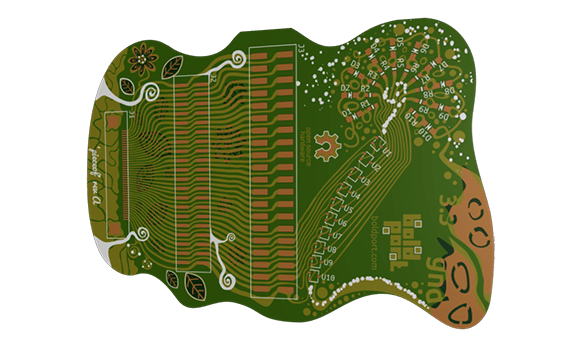
Designing a circuit, laying out a board, and sending it off to be fabbed is so easy anyone can do it. A lot of people are, in fact, and with the traditional tools like KiCAD and Eagle, a lot of different boards look very, very similar. You could always add some cool silkscreen graphics to your board to make it stand out, but [Saar] has a better solution: it’s called PCBmodE, and it allows you to draw circuits artistically instead of the 45° angles we’ve become so accustomed to.
PCBmodE takes the parts, pads, signals, and vias for boards stored in JSON files and converts them to an SVG representation. The file is then routed (manually, but [Saar] is working on automated routing) and Gerberized so it can be sent off to a production house.
You can grab PCBmodE over on bitbucket, but right now it’s still a very early version. Vias and copper pours are working, but [Saar] has only fabbed this board so far.


Great Work..
Even I did something like this to make some home-made keyrings.. Have a look!
http://indiantinker.wordpress.com/2012/10/06/trying-some-graphic-etching/
Oooh. Nice logo there.
Thanks! That is swewed to my old sling bag! :D
I did some blinky LED pins and i had to use curvy lines to fit them in, it turned out quite psychedelic
http://donkey.vernier.se/~ghlargh/temp/mit.gif
So, how about EMC considerations?
I’d be willing to consider them, yes.
When I used to make PCBs at home, before the days of toner transfer and other computer-based methods, I had to manually lay out the tracks on transparency sheets using Bishop Graphics adhesive tape and symbols (such as IC pads) and was able to achieve a similar effect.
Unfortunately, as this person found out at some cost, you can go too far in your search for “artistic” PCBs and actually wreck a solid piece of engineering:
http://folklore.org/ProjectView.py?project=Macintosh&characters=Steve%20Jobs&detail=medium
Great text! That shows exactly that functionality is way more important than the PCB looks.. And by the way, i believe that a well designed PCB is itself a piece of art and craftsmanship.. you don’t need to have curvy traces and assymetrical pads to be ‘artistical’.. just keep it simple and functional
Exactly. Logical art exists too!
The ZX Spectrum, and I’m sure a few other early 80s computers, had swirly tracks and busses all over the PCB. At least the early revision did. Layout hasn’t been done by machines for all that long.
These are engineers talking. From artist point of view its a great challenge to make a board that has some significance for a person who has no techi aestetics. Maybe its not a qiestion of which one is more important but who is making the job and what they are willing to sacrifice to satisfy themselves.
Um 45 Deg? so all your boards are triangles? I like my as squares or rectangles personally…
Don’t you mean octangles? To force a triangle you would need 120deg.
And you should never have 90deg angles on thin traces since it makes it more likely to have etching errors. It also takes up more space to route with 90deg angles than 45deg.
Routing with smooth lines as above is actually ideal, but it’s rarely done since convention says that straight lines and 45deg angles is how you do it.
I tend to think it’s more than just convention. At the very least, I’m willing to bet that it’s easier to create auto-routing routines if you stick to straight lines and angles.
It depends on algorithms you use. Look at “Topor” router.
But why would someone do this? What about EMI, propagation delays, inductance and capacitance between traces?
Propagation delays is nothing most people ever need to bother with, you need to reach the GHz range for that to be a factor.
Capacitance and inductance is mostly a factor of trace length, correctly done smooth traces are shorter than straight traces with sharp corners and should therefore have less inductance and capacitance.
Unless you manage to build a resonant circuit the shape of the trace should not affect EMI, also most people here do hobby designs and don’t have to bother with such.
The only statement that is correct in your reply is “most people do hobby designs and don’t have to bother with such.”
Otherwise the rest of your comments are incorrect and show a lack of any engineering expertise.
OTOH, I’ve heard other engineers say “anything under 1GHz is DC” B^)
Please elaborate instead of just saying “you’re wrong”.
You will not have any problems with propagation delays in low frequency projects like AVR builds.
There are no electromagnetic laws that say smooth curves are bad.
You are right, I should have elaborated more.
My comment was mainly aimed at your ” Propagation delays is nothing most people ever need to bother with, you need to reach the GHz range for that to be a factor.” statement.
Its more than just propagation delays that affect the routing of an effective PCB. I see you’ve clarified your statement with an AVR reference (which don’t go beyount 50Mhz) but careful layout attention must be applied to an oscillator or crystal circuit no matter what frequency they are running. Reset lines, if used, must be routed carefully to avoid random processor resets. Actually, poor handling of your clock circuit or reset line can lead to ramdom processor resets or abnormal program execution.
Bypass and filter capacitors are another frequently overlooked and misunderstood topic.
For the more ambitious crowd, try routing DDR memory lines (ARM processors), which are way under a GHz, artistically without having signal integrity issues, especially with hobbyist friendly double sided boards.
Capacitance and inductance is not just a factor of trace length, but trace width and location to a power plane (or lack of) also have an impact.
The quality of a PCB manufacturing facility also figures, to a lesser degree with hobby type projects, in to the equation.
Didn’t mean to come off all grumpy or superior just understand the consequences when you do something in circuit design just for “looks”.
Well, yes… i was kind of unclear… I meant that in the same environment the capacitance and inductance are just a factor of length. Meaning a rounded trace won’t really affect the inductance and capacitance if routed the same way on the same board.
I wasn’t really thinking DDR traces when i was thinking of most hackaday users, but <40MHz microcontroller IO and serial comm.
Either way. there is nothing but convention that says rounded traces are bad.
“Designing a circuit, laying out a board, and sending it off to be fabbed is so easy anyone can do it”
I disagree — anyone can get a circuit board built, but not every circuit board is easy to design. I guarantee you’d take more than one pass to get a working video board.
I guess that depends a lot on your definition of ‘video board’.
Heh, looks like a TopoR (Topologic Router) from Eremex company. But TopoR is a serious router CAD.
Huh. . . I wonder if the AI is going to take ALL THE JORBS?
Part of me loves this (I am so sick of doing layout) and part of me hates this. It worth trying out, thanks for the link.
This is cool, but PCBs are already art :)
that is beautiful! great work saar!
indeed
Kicad is already considered traditional? Now I feel ancient…
I just want something that can auto route a simple two speed, 12 volt fan controller, with relays and fairly high amp fan motors. I have one built on proto board with all point to point wiring. Works perfectly, looks horrid.
This is absolutely beautiful. Honestly, making a full PCB chain from scratch is a bit of a silly idea if you want to focus on the artistic stuff–I actually think it might be interesting to make an Eagle script or some plugin that would allow you to postprocess or just do normal layout but with nicer curves. IIRC Eagle actually has the functionality to generate really random curved lines, but it’s not an easy interface to do it with.
Hm, maybe not Eagle, but I’m sure there’s some other PCB suite that would work well. Either way, this is a pretty awesome way to look at functional PCB art from the traditional tricks. Yes, the parasitics are not going to be as good, but I think that’s half the challenge–designing a PCB with sufficient electrical performance while still looking beautiful. That is a true intersection of electronics and art–not some PCB in the shape of a business card, and not making some sketchy, unreliable, works-long-enough-to-take-a-video “sewn” electronics with bulky boards sending single ended signals with a craptastic ground (okay, didn’t mean to bash on either, and in fact many business cards and conductive thread designs are quite nice, but my point is. . .this pretty much beats all of them).
Anyway, point is, integration with an existing engineering-oriented PCB layout suite should already permit modelling of the parasitics and make the actual basic electrical layout process much easier.
Not sure why anyone wouldn’t like this. There’s something appealing about adding a unique touch that would only be recognized by other PCB designers. Kind of like an easter egg added to software.
Just art ;)
http://imgur.com/gallery/0Xx14Lg
Author of PCBmodE here. Just a quick note to say thank you for all the comments! I read them all carefully and will take them into account while developing the software.