 It’s time for more blatant advertising for Hackaday Projects, the best project hosting site on the Internet. Did we tell you it’s collaborative? That you and your friends can work on projects together? Want more encouragement to join? How about a contest with prizes that include oscilloscopes, FPGA dev boards, soldering and rework stations, Beaglebones and Raspberries and Spark Cores? Oh my!
Oh. We’re also developing a retrocomputer to show off the features of Hackaday Projects. This is the latest update, showing off the architecture of the entire system, the memory map, and the logic glue and buffers. The plan for this project is to have it host another awesome Hackaday site, our retro version, a small off-shoot of the main Hackaday site that’s specifically designed to be loaded by computers built before 1993. There haven’t been many retro successes in the Hackaday tip line recently, so if you manage to get a vintage computer to pull the retro site up, snap a pic and send it in.
For those of you wanting to catch up on the Hackaday 68k project, here’s the Hackaday Projects page, and here’s all the front page updates. Click that ‘Read more…’ link for the update.
Architecture
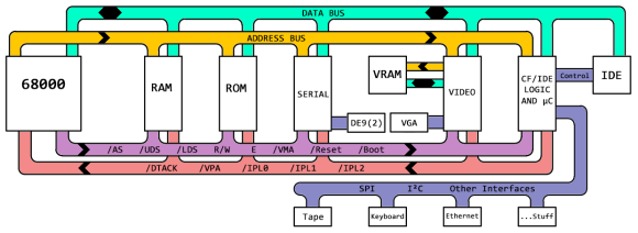
The architecture is actually pretty simple; the CPU, a ton of RAM, 64k ROM, and a pair of 6850 ACIAs (yes, I know, but it’s for a good reason…) giving me two serial ports capable of 19.2 kbps. These four parts are the basic system and are probably the most boring parts of the development.
There will be two or three more cards in the backplane for video, a Compact Flash/IDE adapter, and a microcontroller that will talk to a keyboard, an Ethernet module, a cassette tape drive, and probably some other stuff I haven’t thought of yet. All of these cards are connected via four types of control signals. The address bus is unidirectional, coming out of the CPU card. The data bus is bidirectional.
There are two other groups of control signals, most of which were covered in the last post on this project. Note this isn’t the minimal 68000 system I described in that post. I’ll be using interrupt pins. Because I’m using the 6800 peripheral pins, this means I’ll also need to generate a /DTACK signal. This makes the architecture a little more advanced than the basic, “you can build a 68k system on a breadboard” computer I described in the earlier post, but not by much.
The real fun begins when I get to the video and IDE/microcontroller boards. That’s going to be a Yamaha V9938 Video Display Processor that will have a VGA output and also be compatible with the V9958. This has 128kB of DRAM attached to it, out of the CPU’s address space.
The IDE/Compact Flash/Microcontroller card will provide the control logic for a huge chunk of storage on a CF card, or if I’m feeling extremely adventurous, one of those old-school IBM microdrives hard drives. The IDE spec is a 16-bit wide data bus, so that connects directly to the CPU. This board will also have a PS/2 (or ADB) keyboard port, an Ethernet module, and whatever other cruft I can stuff in there.
Buffers
Here’s a little thought experiment. Connect a LED to one of the address pins on the 68k, kinda like I did in this post. It’ll drive one LED. How about two? Sure. How many more? A dozen? How long until those LEDs stop lighting up?
That’s the problem with connecting the pins on the CPU to RAM, ROM, peripherals, address decoders, and memory logic. Eventually, the CPU won’t be able to drive all the pins. This is why we need buffers and line drivers.
In the last post where I blinked a LED, I was using a simple circuit to drive the LED using a 74HC04 inverter. To drive all the address, data, and control lines, I’ll need something a little more complex. To the surprise of no one, this was a problem solved a long time ago.
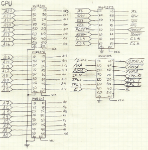
For the unidirectional lines, i.e. the address bus, I’ll be using a 74HC373 octal bus driver. Three of these are dedicated to the address lines, and another two for control signals.
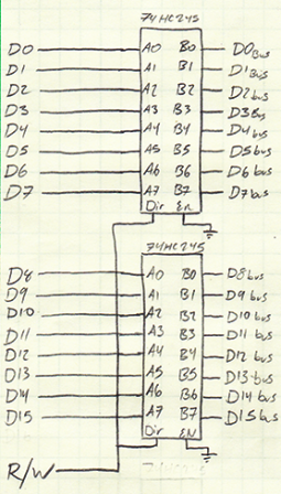
The data line is a little bit trickier. These lines are bidirectional, making the switching a little more difficult, but also a solved problem. The 74HC245 is a bidirectional transceiver, allowing me to connect the data lines from the CPU to one side, the data lines on the backplane to the other, and toggling the direction with the R/W line. Very easy, and a one (or two, technically)-chip solution.
Glue
There’s one last thing before the CPU can access the RAM, ROM, serial port, and all the other stuff that I’m putting in this tiny blue box of an enclosure. The memory and peripheral chips must be decoded into the correct address space. This means using a surprising variety of logic chips to enable reading and writing of everything attached to the CPU.
Before I explain this, I’m going to say yes, I could do this with a CPLD, GAL, or some other type of programmable logic. When this project comes off a wire-wrapped backplane, that’s what I’ll do. With wire-wrapped circuits, everything is extremely easy to modify and you can, theoretically, make an exact duplicate of the schematic just by looking at the wires. Programmable logic is just another point of failure, and I’m doing this the simple way, anyway.
Decoding the RAM and ROM
Generally, all the ‘big’ chips in this project – the video circuitry, RAM, ROM, communications adapters, whatever – will have three pins that need to be toggled: Chip Select, Read, and Write. These pins must be properly selected when the CPU accesses something. Reading and Writing are pretty easy, and selecting each chip only a little more so.
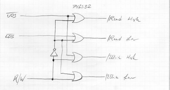
The usual 6502 et al. way of toggling the Read and Write pins on chips is simply connecting the R/W from the CPU to the chip. This line is high when the CPU is reading, and low when the chip is writing. The 68000 has two additional pins for controlling access to chips: /UDS and /LDS. These pins are active (low) when reading or writing to data bits 8-15 or 0-7, respectively. Luckily, the control logic is a simple two-chip solution:
That’s a quad-OR gate and a single inverter taking care of reading or writing to the high (D8-15) or low (D0-7) parts of RAM, ROM, or whatever. Easy, and easily duplicated across multiple cards in the backplane.
Now the fun stuff. Decoding. This is like a puzzle that has surprisingly strict requirements. I need to use a minimal level of gates to turn the address lines into chip select signals to minimize the delay, but I also need to make sure I’m not decoding into unused space in the memory map.
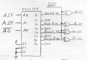 The RAM will be at the bottom of the address space from $000000 to $3FFFF – a full four megabytes. To do this I’m taking 3 to 8 line decoder and attaching the RAM chips to four of the eight outputs. I should note [lennart] over on the Hackaday Projects page came up with a better circuit for RAM decoding. Thanks.
This circuit will put my eight chips of RAM into the address space at $000000 to $3FFFFF with a minimal amount of delay, but there’s a problem: When the 68000 first boots, it looks for instructions at $000000. Since this is RAM, there won’t be any instructions at that position, the computer will halt, and the world will end. I need some sort of circuit to deselect the RAM and select the ROM for the first few clock ticks.
This means I need to generate a /BOOT signal, or a signal that is active (low) for the first eight clock cycles. I’m doing that with a 74HC164 serial in, parallel out shift register, with /BOOT generated from one of the outputs. By putting this signal on the backplane, I can deselect the RAM with some NOR gates, enable the ROM with an OR gate, and have the CPU read some instructions when it’s reset.
A Memory Map
I might as well go over the memory map in this post, so in no particular order, here we go:
- $000000 to $3FFFFF – RAM
- $FF0000 to $FFFFFF – ROM
- 6850 ACIAs are decoded from $EF0040 to $EF0042. ACIA 1 is even, ACIA 2 is odd. More on that later.
- V9938 is at $DF0000 and $DF0001 for Mode 0 and Mode 1, respectively.
Noticing a pattern with the peripherals? I’m taking the top eight bits of the address space and changing one bit for each peripheral. This simplifies the decoding, as I can use a single 74HC30 eight-input NAND gate for the RAM, and add a single inverter to an address line to decode all the peripherals. Simple, fast, and easily modified and copied across the entire system. This setup of changing one or two of the top four address bits for each part of the system also has another benefit: It’s easy to tell which peripheral is being accessed by putting LEDs on the top four address bits just like I did with the last post.
That’s it for this update, and it unfortunately describes the system well enough that there’s nothing to update until I get a ROM monitor and serial port running on this system. Good news, though: [Bil Herd], creator of the Commodore 128, the cheaper 8-bit Commodores, and generally awesome dude will be making an appearance in the next update.
This is the boring part of system construction. Don’t get me wrong; getting a minimal system running is rewarding, but the real fun in this project is going to happen when I get to the video circuitry, IDE hard drive, microcontroller, and all those crazy peripherals working. After that, it’s even more fun with getting an OS and compiler running. I actually have an idea for an OS that has never been done before, and is still only a twinkle in the eye of the BeOS and Haiku OS designers. That might take a year or two.
Updates to follow, and until then follow this on Hackaday Projects.






I wouldn’t bother with the *slooow* 68XX peripherals as it is trival to use the 80xx peripherals. e.g. 8155, 8255 and 16×50 UART (PC16550DN in DIP) with large FIFO etc.
Writing monitor and serial bootloader/flashers in C are fun.
If you can interface to EPROM/FLASH chips, you can interface to 80XX peripherals chips. Same type of bus cycles, just have to pick a right speed grade.
Oh, that takes me back. In the 90’s, we always had to check to see if our serial ports had 16550 UARTs so they could handle the “high speed” modems we used. As a BBS sysop, this was particularly important to me. You just can’t run a 28.8k modem on a slow port.
…Feeling old…
I’d suggest using a 74hc541 as a buffer instead of the 74hc373 you’ll find the pin out much easier to do a layout with when you want to switch to PCB
Or 74xx573 for the transparent latch in “Flow Through” pin out.
If you want octal buffer buffers, just use the old 74XX245 and fix the /DIR level – reuse same parts to take advantage of quantity discount or inventory etc
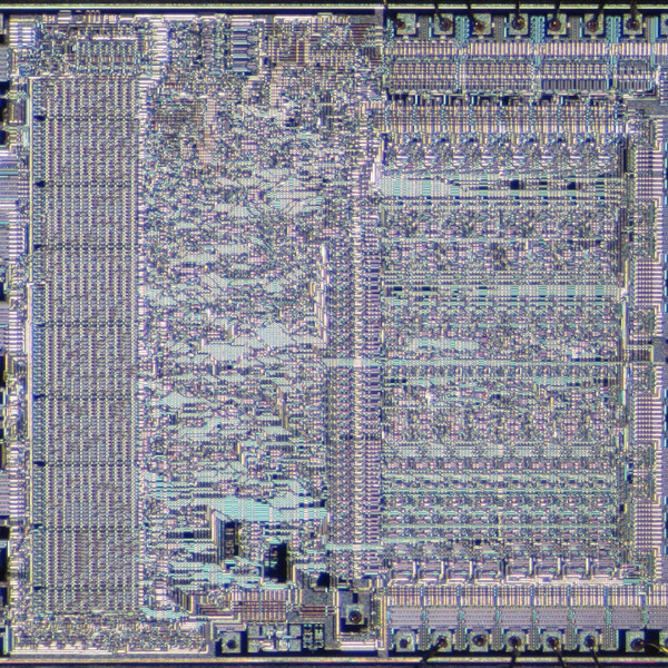
That chip you used for your graphic looks like a classic. They haven’t made anything like that since the mid 1970s. With the purple ceramic and the gold stripe.
Unfortunately I’m using a boring, plastic DIP for the real one. If I could find an HC purple ceramic version, though…
I happen to have a couple 10mhz 68k processors in gold plated cerdips in my collection…
I think I do too.
Does anyone know the reason behind the gold stripe? I’ve wondered for some time and I can’t seem to find the right phrase to Google.
I think it’s a bit like a PCB trace, and it connects the lid of the package to ground.
I definitely want to see the details on how to get VGA out of the V9938. The horizontal rate is that of NTSC and many VGA monitors won’t sync that low. From my own futzing about with the V9838, it seems straightforward to connect a RAMDAC via the (thoughtfully provided) colorbus. Its just that darned horizontal rate that makes me wonder if I should bother. Hoping you have another approach.
I cheat and use a NTSC to VGA converter. I use one with a TMS9918 with good results.
This is really unlikely to be generally applicable, but I was pleasantly surprised when I discovered my LCD desktop monitors happened to know how to sync to 720×240@60 (“NTSC”) and 720×288@50 (“PAL”) over VGA. They’re Acer G215Hs, so maybe other Acer monitors can do the same.
I bought a $120 1080 “LED” TV as my second monitor. It supports HDMI/VGA/component/S-video/Composite input. :)
What is the purpose of locating the RAM at $000000 and the ROM $FF0000 and doing all of that nonsense with the 74HC164, NOR and OR gates? Swap RAM/ROM locations and let the assembler figure out where to point the jumps, branches or whatever at.
Having RAM at 0000xxxx allows to change the interrupt and exception vectors after boot is done. Otherwise, you set them in the ROM and they always jump at a fixed address, which is slightly less useful.
Also, it’s “Haiku”, not “Haiku OS”. As an Haiku developper, I have to complain about this, until everyone gets it right… (and yes, we know even our domain name is wrong).
My guess would be that he’d like to modify the exception table (which resides at $0) later. With ROM there, it’d be hardcoded. Yes, you could fill all exceptions with jumps to RAM, but that’d add latency to your interrupts.
^ that or you want to use a bootstrap loader to load RAM with your ROM code at that location to speed up your development cycle. Having to Erase, then Program just to change a few bytes can take a while for FLASH and EPROM.
I made a 8031 development board that can remap the RAM to ROM at a different address space for that reason. The monitor bootstrap loads the code to RAM, remaps the address decoder. The hardware reset to the new “ROM”, but you can reboot to monitor if you hold down the reset longer than 3 seconds or a power cycle.
Nice, detailed post! For what it’s worth, though, when you’re trying to emphasise the collaborative aspects of HaD projects, you probably shouldn’t write the whole post in first-person. :)
Hi, I think decodinge ram and ron schema is wrong. /Write low musn’t be connected to /LDS ?
Cassete player? You hipster! :p And this is the interesting part IMO, not fun but interesting.
very interesante my fried
Lemme see… I think I still have my Commodore 64 Cassette player somewhere…
hi
any news about this great project ?
any repo about the V9938 ?
i have developed a filesystem and a little monitor, in C, and i have been developing a 68000 board, so i’d like to integrate things