A few years ago [Ben Krasnow] built a scanning electron microscope from a few parts he had sitting around. He’s done a few overviews of how he built his SEM, but now he’s put up a great video on how to control electrons, focus them into a point, and scan a sample.
The basic idea behind a scanning electron microscope is to shoot electrons down a tube, focus them into a point, and scan a conductive sample and detect the secondary electrons shot off the sample and display them on an oscilloscope. [Ben] is generating electrons with a small tungsten filament at the top of his electron ‘stack’. Being like charged, these electrons naturally fan out, so a good bit of electron optics are required to get a small point.
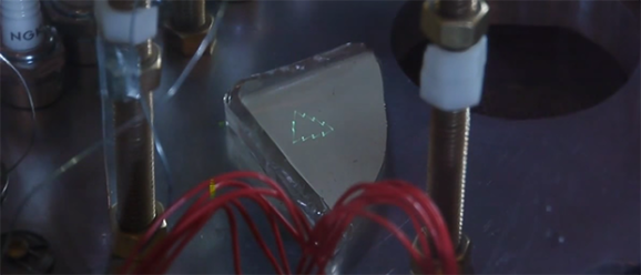
Focusing is done through a series of pinholes and electrostatic deflectors, much like you’d see in an old oscilloscope CRT. In the video, you can see [Ben] shooting electrons and displaying a Christmas tree graphic onto a piece of phosphor-coated glass. He has a pretty big scanning area in his SEM, more than enough to look at a few chips, wafers, and whatever other crazy stuff is coming out of [Ben]’s lab.
Video below, along with the three-year-old overview of the entire microscope.


http://benkrasnow.blogspot.com.au/2014/04/electron-beam-control-in-scanning.html
At least jump to his blog for this, he deserves the traffic!
Thanks, added.
I’m afraid to click this link, because I have a load of work to do and I know if I click this I’ll be watching cool videos for the next 5 hours, bookmarked for the weekend ;)
Very interesting, but now I’m half an hour late.
Brian Benchoff,
Do you plan on posting instructions along with a parts list so someone like me can build one?
I don’t.