Converting A Scanning Electron Microscope Into A TEM Is Surprisingly Easy

Although both a SEM and a TEM are electron microscopes, their working principles and images are very different. Whereas an SEM uses secondary electrons ejected after bombarding a sample’s surface with primary electrons, a TEM works more like an X-ray machine, with a sensor placed behind the sample to record primary electrons after they pass through said sample. It is, however, possible to turn a SEM into a TEM with some creativity, as [ProjectsInFlight] recently did with his SEM.

We previously covered how the SEM in the video was saved from being scrapped and subsequently revived, and now it is getting a pretty nice upgrade. That said, this SEM to TEM change isn’t anything new, with so-called STEM imaging having been possible for ages using a rather simple reflecting adapter. The problem here is that such adapters cost enough to make you dread filing a budget request, yet they are simple enough that you might be able to DIY one.

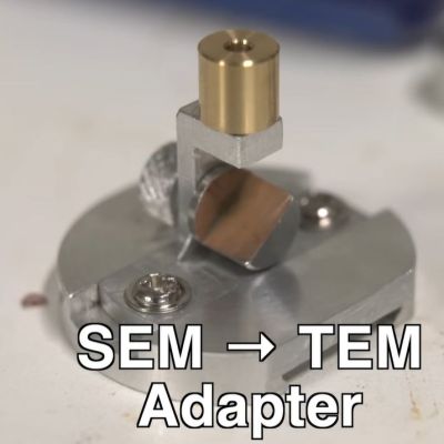
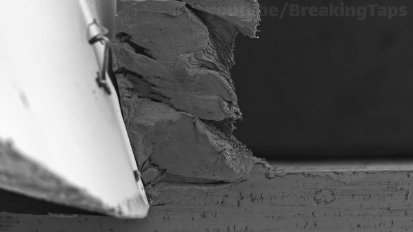
The main concern with the DIY adapter was clearance between the sample holder and the fragile components inside the chamber. This turned out to be a hair under 14 mm (0.55″), giving not a lot of space to work with, but that was relative to the standard bulky sample holder. With a thinner sample plate machined out of aluminum, significantly more space became available, including for the primary electron mirror and shield for the secondary electrons.

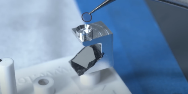
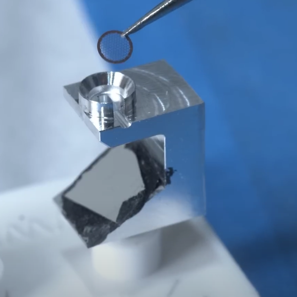
Some more lathe, milling, and tapping work later, the entire sample holder came together. During testing a hack was implemented to enable adjusting the mirror angle while in the evacuated vacuum chamber so that the adapter could be dialed-in. Subsequently, a first sample was imagined in the form of gold nanoparticles, which revealed a leaky secondary electron shield due to bypassing.

Further testing revealed that the shield needed to extend much higher to meaningfully block secondary electrons, after which the TEM image massively improved. Subsequently, a previously expired mosquito graciously donated its wings to science, with TEM imaging clearly revealing the delicate structures within these wonders of evolutionary design.

The next challenge will be to TEM image biological cells, which require substantial preparation.

This isn’t the first STEM converter we’ve seen. The SEM has a long checkered history that we’ve talked about before, too.

Continue reading “Converting A Scanning Electron Microscope Into A TEM Is Surprisingly Easy”

The green CRT display of a scanning-electron microscope is shown, displaying small particles.

DIY Calibration Target For Electron Microscopes

It’s a problem that few of us will ever face, but if you ever have to calibrate your scanning electron microscope, you’ll need a resolution target with a high contrast under an electron beam. This requires an extremely small pattern of alternating high and low-density materials, which [ProjectsInFlight] created in his latest video by depositing gold nanoparticles on a silicon slide.

[ProjectsInFlight]’s scanning electron microscope came from a lab that discarded it as nonfunctional, and as we’ve seen before, he’s since been getting it back into working condition. When it was new, it could magnify 200,000 times and resolve features of 5.5 nm, and a resolution target with a range of feature sizes would indicate how high a magnification the microscope could still reach. [ProjectsInFlight] could also use the target to make before-and-after comparisons for his repairs, and to properly adjust the electron beam.

Since it’s easy to get very flat silicon wafers, [ProjectsInFlight] settled on these as the low-density portion of the target, and deposited a range of sizes of gold nanoparticles onto them as the high-density portion. To make the nanoparticles, he started by dissolving a small sample of gold in aqua regia to make chloroauric acid, then reduced this back to gold nanoparticles using sodium citrate. This gave particles in the 50-100 nanometer range, but [ProjectsInFlight] also needed some larger particles. This proved troublesome for a while, until he learned that he needed to cool the reaction temperature solution to near freezing before making the nanoparticles.

Using these particles, [ProjectsInFlight] was able to tune the astigmatism settings on the microscope’s electron beam so that it could clearly resolve the larger particles, and just barely see the smaller particles – quite an achievement considering that they’re under 100 nanometers across!

Electron microscopes are still a pretty rare build, but not unheard-of. If you ever find one that’s broken, it could be a worthwhile investment.

Continue reading “DIY Calibration Target For Electron Microscopes”

Getting A Close-Up View Of Chip Formation With An SEM

When all you’ve got is a hammer, everything looks like a nail. And when you’ve got a scanning electron microscope, everything must look like a sample that would be really, really interesting to see enlarged in all its 3D glory. And this is what [Zachary Tong] delivers with this up close and personal look at the chip formation process.

We’ve got to hand it to [Zach] with this one, because it seems like this was one of those projects that just fought back the whole time. Granted, the idea of cutting metal inside the vacuum chamber of an SEM seems like quite an undertaking right up front. To accomplish this, [Zach] needed to build a custom tool to advance a cutting edge into a piece of stock by tiny increments. His starting point was a simple off-the-shelf linear stage, which needed a lot of prep work before going into the SEM vacuum chamber. The stage’s micrometer advances a carbide insert into a small piece of aluminum 50 microns at a time, raising a tiny sliver of aluminum while it slowly plows a tiny groove into the workpiece.

Getting the multiple shots required to make a decent animation with this rig was no mean feat. [Zach]’s SEM sample chamber doesn’t have any electrical connections, so each of the 159 frames required a painstaking process of advancing the tool, pulling down a vacuum in the chamber, and taking a picture. With each frame taking at least five minutes, this was clearly a labor of love. The results are worth it, though; stitched together, the electron micrographs show the chip formation process in amazing detail. The aluminum oxide layer on the top of the workpiece is clearly visible, as are the different zones of cutting action. The grain of the metal is also clearly visible, and the “gumminess” of the chip is readily apparent too.

For as much work as this was, it seems like [Zach] had things a bit easier than [Ben Krasnow] did when he tried something similar with a much less capable SEM.

Continue reading “Getting A Close-Up View Of Chip Formation With An SEM”

Building An Electron Microscope For Research

There are a lot of situations where a research group may turn to an electron microscope to get information about whatever system they might be studying. Assessing the structure of a virus or protein, analyzing the morphology of a new nanoparticle, or examining the layout of a semiconductor all might require the use of one of these devices. But if your research involves the electron microscope itself, you might be a little more reluctant to tear down these expensive devices to take a look behind the curtain as the costs to do this for more than a few could quickly get out of hand. That’s why this research group has created their own electron detector.

Specifically, the electron detector is designed for use in a scanning electron microscope, which is typically used for inspecting the surface of a sample and retrieving a high-resolution, 3D image of it compared to transmission microscopes which can probe internal structures. The detector is built on a four-layer PCB which includes the photodiode sensing array, a series of amplifiers, and a power supply. All of the circuit diagrams and schematics are available for inspection as well thanks to the design being licensed under the open Creative Commons license. For any research team looking to build this, a bill of materials is also included, as is a set of build instructions.

While this is only one piece of the puzzle surrounding the setup and operation of an electron microscope, its arguably the most important, and also greatly lowers the barrier of entry for anyone looking to analyze electron microscope design themselves. With an open standard, anyone is free to modify or augment this design as they see fit which is a marked improvement over the closed and expensive proprietary microscopes out there. And, if low-cost microscopes are your thing be sure to check out this fluorescence microscope we featured that uses readily-available parts to dramatically lower the cost compared to commercial offerings.

Machine Learning Helps Electron Microscopy

Machine learning is supposed to help us do everything these days, so why not electron microscopy? A team from Ireland has done just that and published their results using machine learning to enhance STEM — scanning transmission electron microscopy. The result is important because it targets a very particular use case — low dose STEM.

The problem is that to get high resolutions, you typically need to use high electron doses. However, bombarding a delicate, often biological, subject with high-energy electrons may change what you are looking at and damage the sample. But using reduced electron dosages results in a poor image due to Poisson noise. The new technique learns how to compensate for the noise and produce a better-quality image even at low dosages.

Continue reading “Machine Learning Helps Electron Microscopy”

Electron Microscope Conversion Hack

Some of you probably know this already, but there’s actually more than one kind of electron microscope. In electronics work, the scanning electron microscope (SEM) is the most common. You hit something with electrons and watch for secondary electron emissions. However, biologists more often use a TEM — a transmissive electron microscope — which passes electrons through a sample to image it. [Breaking Taps] built a small device to convert his SEM into a TEM.

One key idea is that in a SEM, the beam’s position on the target is the only thing that matters. Any secondary electron detected is a result of that spot’s composition, no matter where you collect them. Common detectors pick up back-scattered electrons bouncing back toward the electron source.  There are also low-energy electrons bouncing off in random directions, depending on the topology of the target.

The slow electrons can be attracted by a single detector that has a strong positive charge. TEM  doesn’t detect secondary electron emissions. Instead, it passes electrons through a target and collects the ones that pass through a very thin sample using a screen that glows when electrons hit it.

The idea, then, is to create a STEM-SEM device. There’s a sample holder and an angled reflector that shoots electrons passing toward the SEM’s detector. The back-scatter detector is not used, and a shield prevents the detector from seeing secondary emissions from the target itself.

You can buy these, but they are well over $1,000, so in true hacker fashion, [Breaking Taps] made his own.  You could, too, but you’d need a pretty good machine shop and — oh yeah — a scanning electron microscope.

While we have seen some home labs with electron microscopes, you need some high-tech vacuum and high-voltage gear, so it isn’t too common. Armed with a STEM, you can even see the shadows of atoms.

Continue reading “Electron Microscope Conversion Hack”

Viewing Atoms With Electrons

When we were in school, they always told us we can’t see atoms. If you have an electron microscope, then they were wrong. [AlphaPhoenix] has access to a scanning tunneling transmission electron microscope and he shows us some atoms in a very thin slice of a crystal.

Of course, you aren’t directly imaging the atoms. You are looking at the shadows of the atoms, but still. If you’ve never worked with a SEM or STEM before, there are plenty of little details that are interesting like the sample holders and the vacuum system.

Continue reading “Viewing Atoms With Electrons”